By Brian Dipert
Editor-In-Chief
Embedded Vision Alliance
Senior Analyst
BDTI
A diversity of image sensor options are available for your consideration, differentiated both in terms of their fundamental semiconductor process foundations and of their circuit (and filter, microlens and other supplement) implementations. Understanding their respective strengths and shortcomings is critical to making an appropriate product selection for your next embedded vision system design.
The image sensor is a critical part of an embedded vision system, since it's at this initial stage of the hardware design that light photons transform into digital 1s and 0s for subsequent processing and analysis. It's not the first stage, mind you; ambient light (in some cases augmented by an integrated LED flash module or other auxiliary illumination source) must first pass through the optics subsystem. However, BDTI engineer Shehrzad Qureshi already tackled the optics topic with aplomb in his article Lens Distortion Correction.
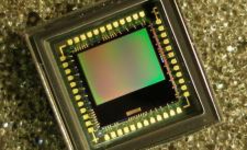
The fundamental purpose of the image sensor, an increasingly prevalent semiconductor device found in digital still and video cameras, mobile phones and tablets, the bezels of laptop and all-in-one computers along with standalone displays, game console peripherals, and other systems, is to approximate the photon-collecting capabilities of the human eye's retina:
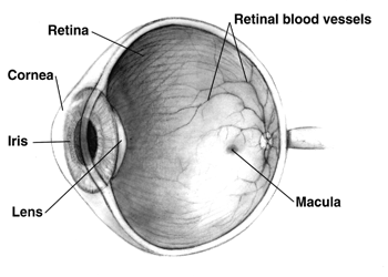
If your system needs to only work with black-and-white images, an elementary image sensor (often augmented by an infrared light-blocking filter) may suffice, mimicking the function of the retina's rod photoreceptors. However, many embedded vision systems benefit from (if not require) the capture of full-color frames. The retina contains three kinds of cones with different photopsin chemical compositions, which have different response curves reflective of their differing responses to a full-spectrum color source.
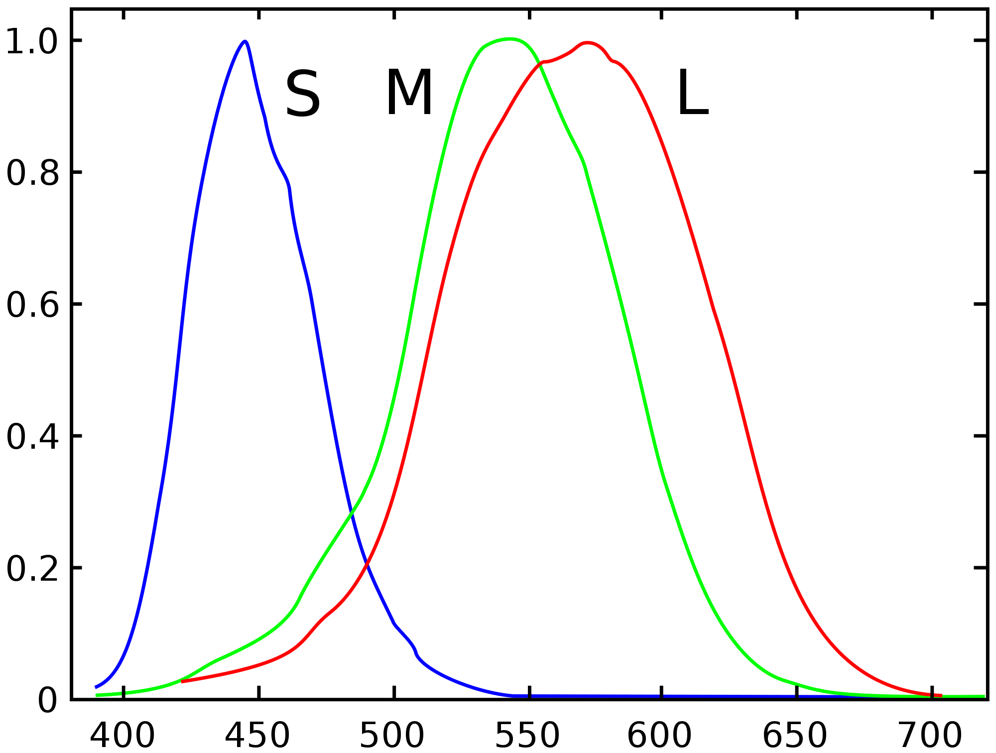
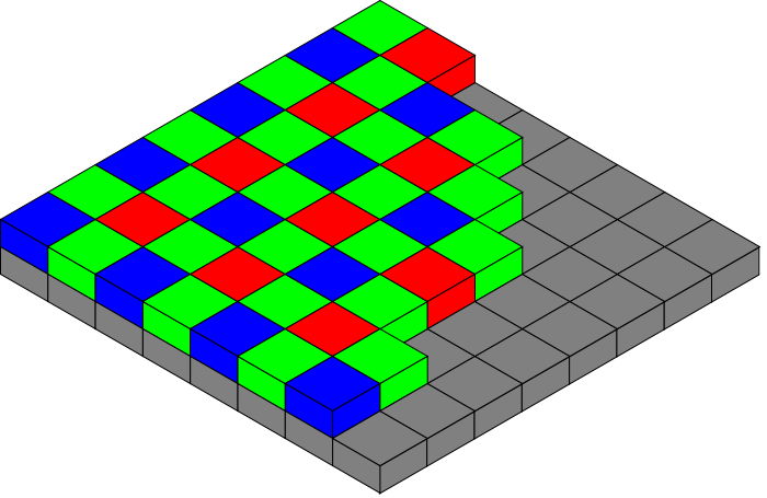
With the exception of some color-blind individuals, for whom one or multiple sets of cones have diminished-to-completely absent function, most humans therefore have trichromatic vision (conversely, a few rare individuals possess four or more distinct cone types). The presence of a multi-color filter array on top of the image sensor's pixel array structure is intended to mimic the retina's L (long: red-dominant), M (medium: green-dominant) and S (short: blue-dominant) cone suite. Due in part to the spectral overlap between M and S cones, evolutionarily explained as enabling early humanoids to discern both potential predators and prey in an overhead foliage canopy, the human visual system is disproportionally sensitive to detail in green spectrum light. Therefore, the Bayer pattern filter array (named after Eastman Kodak's Bryce E. Bayer, its inventor) contains twice as many green filters as either red or blue:
Post-capture processing approximates full-spectrum data for a blue-filter pixel, for example, by interpolating the red- and green-filtered information gathered by nearest-neighbor pixels. Other multi-color combinations are also possible. More recent Kodak sensors, for example, supplement red, green and blue filters with panchromatic (clear) ones in various proportions and patterns, trading off resolution accuracy for improved low-light performance. Subtractive color (CYM, for cyan, yellow and magenta) filter combinations are also possible. And JVC's first-generation GR-HD1 (consumer) and JY-HD10 (professional) HDV camcorder even employed a hybrid complementary/primary matrix of clear, green, cyan, and yellow filters.
The Foveon-championed X3 approach is also of interest in this regard (Foveon is now owned by Sigma, its long-standing primary camera customer). X3 sensors rely on the variable-depth absorption of various light frequencies within a semiconductor foundation. Successively located photodiodes capture the red, green and blue spectrum specifics within each pixel's surface-area dimensions:
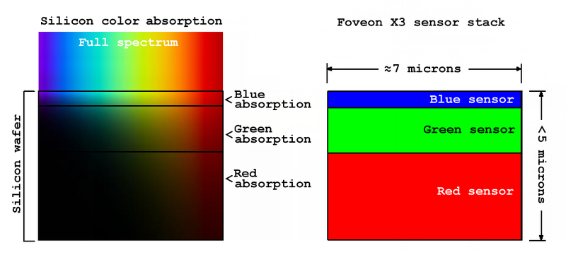
leading to same-pixel-location capture of red, blue and green spectrum information with no need for interpolation-induced approximation (and consequent arguably-visible artifacts). X3 sensors tend to deliver lower pixel site counts than do conventional Bayer- or other-pattern filter array-based sensors, but supporters claim that their more accurate 'film'-like reproduction of captured images more than makes up for any raw resolution shortcoming.
CCDs versus CMOS image sensors
Until relatively recently, the CCD (charge-coupled device) was the conventional silicon foundation for image sensors, and it remains the technology of choice for some applications. Electron charge packets accumulate in potential wells; CCDs' 'global shutter' approach terminates this accumulation for all pixels at the same point in time, with charge values sequentially read out of the device in a serial manner and converted from the analog to digital domain via external circuitry:
CCDs still find use in ultra-high-resolution applications, and in ultra-low-light environments such as astrophotography. However, they are also power-hungry and require custom semiconductor processing that has proven to be increasingly expensive versus the conventional bulk CMOS alternative and also limits the amount of beyond-sensor circuitry that can be integrated on a single sliver of silicon. Conversely, CMOS image sensors (as is the case with solar cells) are capable of being manufactured on mature, already-amortized semiconductor fabs that previously produced leading-edge RAMs, FPGAs, processors, and the like.
Therefore, the ascendant CMOS sensor quickly achieved widespread adoption once the resolution it could cost-effectively deliver became acceptable for volume applications. As Wikipedia concisely notes:
APS pixels solve the speed and scalability issues of the passive-pixel sensor. They generally consume less power than CCDs, have less image lag, and require less specialized manufacturing facilities. Unlike CCDs, APS [active-pixel] sensors can combine the image sensor function and image processing functions within the same integrated circuit; CMOS-type APS sensors are typically suited to applications in which packaging, power management, and on-chip processing are important.
CMOS sensors' pixel locations are capable of being randomly accessed. The sensors commonly come in two-, three- and four-transistor per-pixel circuit configurations:

Two-Transistor Circuit

Three-Transistor Circuit
While 'global shutter' CMOS sensors have been demonstrated in prototype form, the 'rolling shutter' alternative architecture is dominant (if not universal) with production devices. With it, each pixel row's worth of data sequentially transfer to a buffer register prior to pixel line reset; the buffered (and subsequently A/D-converted) information then passes to the system processor via external I/O cycles. The advantage of this line-scan approach is reduced silicon overhead versus the 'global shutter' alternative, which would require an incremental multi-transistor and light-blocked circuit structure within each pixel to store the accumulated-photon value. The rolling shutter downside, on the other hand, is that different regions of the sensor capture the image at different points in time, leading to objectionable distortion artifacts with fast-moving subjects:

Wobble

Skew

Smear

Partial Exposure
Pixel pitch issues
Large-pixel conventional image sensors often require anti-aliasing filters ahead of them. The anti-aliasing filter serves an analogous process to its audio processing counterpart; it slightly "blurs" the image captured by the sensor in order to compensate for optics-enabled spectral response significantly above the Nyquist frequency of 1/(2*pixel spacing). Aliasing often appears as a Moiré pattern on image regions containing high-frequency repetition, such as window screens and tight texture patterns. Alternative pixel structures such the earlier-mentioned Foveon sensor have less need for resolution-reducing anti-aliasing, as is the case with conventional sensors as their individual pixels decrease in size.
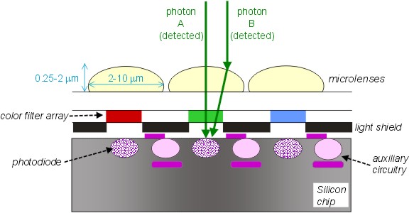
Moore's Law-driven pixel dimension shrinks enable cost-effective delivery of increasing image resolution over time, however they also degrade the sensor's low-light sensitivity by constricting each pixel's ability to collect sufficient photon data in a given amount of time. This undesirable tradeoff is particularly evident with low-fill-rate designs, in which the photodiode comprises a small percentage of each pixel's total surface area:
As partial compensation, manufacturers often place a micro lens array on top of the sensor:
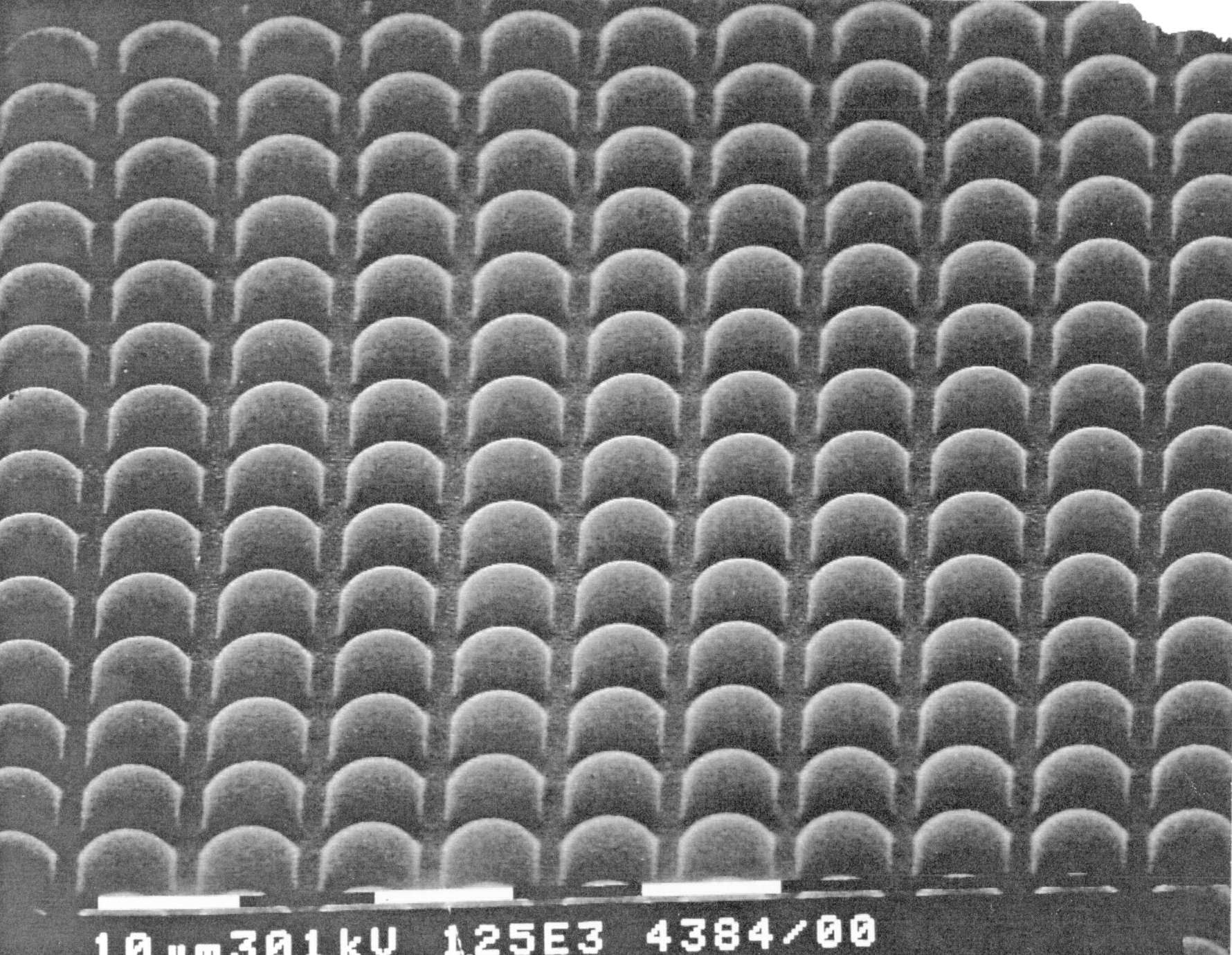
By “bending” the light as it strikes the sensor, each micro lens enables its correlated photodiode to capture more photon information:
Future articles in this series will discuss methods of compensating for various image sensor limitations (low-light SNR issues, de-mosaic interpolation artifacts, micro-lens-induced color filter errors, etc.), as well as the image processor (the next notable link in the embedded vision chain) and the various available schemes for interconnecting the sensor and processor.