
This article was originally published at Lattice Semiconductor's website. It is reprinted here with the permission of Lattice Semiconductor.
The rapid rise in the number of sensors that are being integrated into the current generation of embedded designs, as well as the integration of low cost cameras and displays, have opened the door to a wide range of exciting new intelligence and vision applications. At the same time, this embedded vision revolution has forced designers to carefully re-evaluate their processing needs. New, data-rich video applications are driving designers to reconsider their decision to use a particular Applications Processor (AP), ASIC or ASSP. In some cases, however, large software investments in existing APs, ASICs or ASSPs and the high startup costs for new devices prohibit replacement. In this situation, designers are looking for co-processing solutions that can provide the added horsepower required for these new, data-rich applications without violating stringent system cost and power limits.
Additionally, the widespread adoption of low cost, mobile-influenced MIPI peripherals has created new connectivity challenges. Designers want to take advantage of the economies of scale the latest generation of MIPI cameras and displays offer. But they also want to preserve their existing investment in legacy devices. In this rapidly evolving landscape, how can designers address the growing interface mismatch between sensors, embedded displays and APs?
What designers need is a highly flexible solution that offers the logic resources of a high performance, “best-in-class” co-processor capable of highly-parallel computation that is required in vision and intelligence applications, while adding high levels of connectivity and support for a wide range of I/O standards and protocols. Moreover, this solution should offer a highly scalable architecture and support the use of mainstream, low-cost external DDR DRAM at high data rates. Finally, this device should be optimized for both low power and low-cost operation, and offer designers the opportunity to use industry- leading, highly compact packages.
In the following sections, we will introduce the ECP5™ and LatticeECP3™ FPGAs as viable solutions to overcome embedded design co-processing and connectivity challenges, and highlight application examples at the edge in industrial, consumer, automotive and machine learning areas, where these FPGAs solve the above mentioned challenges.
Efficient Co-processing for Vision and Intelligence
To address the need for a best-in-class co-processor with high level of connectivity and optimized for low-power and low-cost, Lattice Semiconductor® developed the ECP5 and LatticeECP3 FPGA families. Featuring densities of up to 85K look up tables (LUTs) in the industry’s smallest package (10×10 mm) with SERDES, the ECP5 family packs almost 2x the functional density of competitive solutions in a compact footprint, at a fraction of the cost and significantly lower power consumption. These FPGAs support connectivity to ASICs, ASSPs and APs with an optimized I/O and routing architecture. Enhanced embedded DSP blocks and a highly parallel FPGA logic fabric offer greatly efficient performance for compute-intensive co-processing functions. The ECP5 family also adds up to 4 channels of SERDES connectivity, including support for PCI Express (Gen1, Gen2), Ethernet (1GbE, SGMII, XAUI), CPRI, Embedded Display Port (eDP) and JESD204B to deliver data rates from 250 Mbps to 5 Gbps per channel. And programmable I/Os support a wide range of interfaces including DDR3, LPDDR3, LVCMOS, RGMII, XGMII, LVTTL, LVDS, Bus-LVDS, 7:1 LVDS, LVPECL and MIPI D- PHY .
When co-processing or connectivity applications require more than 85K LUTs or more than 4 SERDES channels, designers can turn to LatticeECP3 FPGAs. This product line offers up to 150K LUTs and up to 6.8 Mbits of SRAM in a variety of packages as small as 10×10 mm. These complementary devices to the ECP5 family support up to 16 SERDES channels capable of 3.125 Gbps. Each device supports 800 Mbps DDR3 and LVDS. Over 500 programmable sys I/O buffers help support Ethernet (over RGMII and XGMII) and a host of additional I/O interfaces, while embedded SERDES supports PCIe, Ethernet (over SGMII and XAUI), HDMI, Serial Rapid I/O, CPRI, JESD204A/B and more. Power consumption on the LatticeECP3 family runs as low as 0.5 W. As with the ECP5 family, designers using LatticeECP3 devices can efficiently perform compute- intensive functions using the highly parallel FPGA logic fabric and reduce processor workload by offloading vision and intelligence functions such as image processing and analytics into the FPGA, resulting in lower power and higher performance.
Vision Processing in Industrial Applications
In the industrial arena, ECP5-based co-processing can play an important role by reducing the computational load on the AP, ASIC, or ASSP in video camera, surveillance and machine vision applications. Figure 1 depicts a typical industrial video camera application. Here the FPGA sits between an image sensor and an Ethernet PHY. The image sensor inputs the image data stream to the FPGA, which then performs image processing functions or image compression using H.264 encoding. The FPGA’s on-chip Embedded Block RAM (EBR) and DSP blocks enable high performance Wide Dynamic Range (WDR) and image signal processing (ISP) capabilities. Finally, the FPGA sends the image out to the Ethernet network.
Figure 1. By performing image processing or compression functions, the ECP5 FPGA can reduce the computational load on the AP in industrial video camera applications.
In addition to image processing and compression, the FPGA can also perform video-bridging functions if the type or number of available interfaces on the AP does not match the needs of the image sensor or sensors. To address the needs for flexible connectivity in industrial applications, Lattice offers an ECP5 12K device with programmable support to bridge popular interfaces including LVDS, MIPI and LPDDR3. This device integrates a cost-optimized mix of logic, memory and DSP resources to address both pre- and post-processing needs in applications such as LED controllers, machine vision systems and industrial motor control.
Other than general industrial camera applications discussed above, machine vision, a more specialized camera application in the industrial space, can also benefit from ECP5’s connectivity and co-processing capabilities. The block diagram below in Figure 2 illustrates the wide variety of roles FPGAs can play in a typical industrial machine vision system. On the camera side, FPGAs can serve as a sensor bridge, act as a complete camera ISP, or perform custom functions to help system designers achieveend-product differentiation. On the frame grabber board, FPGAs like the ECP5 can handle video interface and image processing functions.
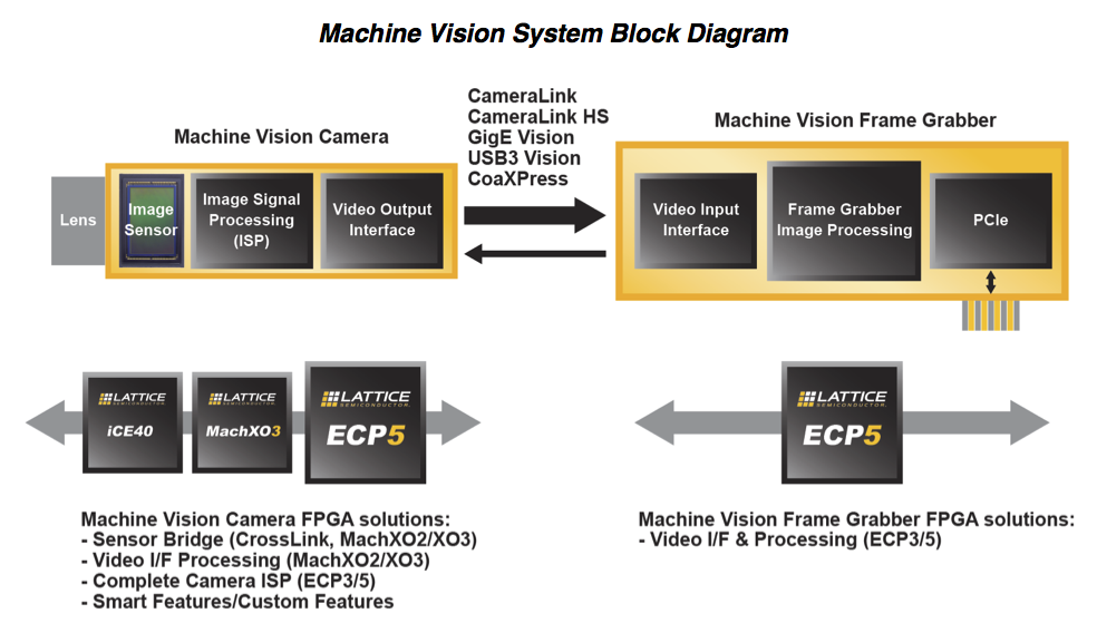
Figure 2. In a typical industrial machine vision solution, FPGAs can perform a variety of interfacing and processing functions.
Intelligent Cameras for Traffic and Surveillance in Smart Cities
Intelligent traffic systems (ITS), including traffic flow monitoring, traffic violations identification, smart parking, and toll collection are a key part of the vision of smart cities. Such systems typically require intelligent traffic cameras that can accurately detect many aspects of a vehicle, such as license plates, even in harsh environments, to perform video analytics at the Edge, rather than sending raw video streams back to the Cloud. An AP alone often cannot meet the real-time processing requirements while staying within the system’s power budget. The ECP5 family of low-power, small form factor FPGAs, acting as a co-processor to the AP, can enable efficient real-time processing at the Edge required by such systems.
In addition to ISP functions mentioned in previous section, the ECP5 FPGA can also perform video analytics functions to further off-load compute-intensive functions from the AP, resulting in lower system power and higher real-time performance. An intelligent camera would utilize the FPGA for object detection, image processing, and image enhancement. The object detected, for example, can be faces in a surveillance camera use-case, or license plates in a traffic camera use-case.
Figure 3. Intelligent camera block diagram where an ECP5 FPGA is performing both image processing and video analytics functions, off-loading compute intensive functions from the application processor.
In the intelligent traffic camera example shown in Figure 3, the FPGA detects the vehicle license plate from an image received from the sensor, performs image enhancement to generate clear images even in low-light or strong backlight conditions – by using different exposure settings for the object (license plate) vs. the background (rest of the image), and fuses the object and the background images to create a clear picture. The FPGA’s object detection result is input into the analytics algorithm running on the AP. By off-loading the most compute-intensive steps in the analytics algorithm into the ECP5 FPGA’s parallel-processing fabric, the intelligent camera is able to increase performance while maintaining power efficiency.
Enabling Immersive Augmented Reality (AR) & Virtual Reality (VR) in Mobile Systems
As the market need for AR/VR environments continues to grow, current head mounted display (HMD)-based systems witness performance issues running content on mobile APs. As such, performing visual based positional tracking, required for an immersive AR/VR experience, has proven challenging on the processor. Here, the efficient parallel-processing architecture of ECP5 FPGAs are well-suited for enabling positional tracking using stereo camera and LED markers. The FPGA offers lower latency and increased power-efficiency image processing compared to an AP. The programmable fabric and I/Os of the FPGA also allow system designers to easily choose and source the camera sensor from different vendors based on the product requirement.
In “outside-in” positional tracking a stereo camera is placed in the room (looking outside-in from room environment toward the user) to track user movements – such as body motions and hand movements – via LED markers mounted on headset and hand controllers, as shown in Figure 4 below. The FPGA, located inside the camera unit on the tripod, uses the stereo camera data to calculate user’s position, body motions and hand movements, which is then wirelessly passed on to the mobile AP (located in the HMD) to be incorporated into the AR/VR application. The use of stereo camera provides depth perception to the algorithms running on the FPGA, enabling positional tracking in all three dimensions.
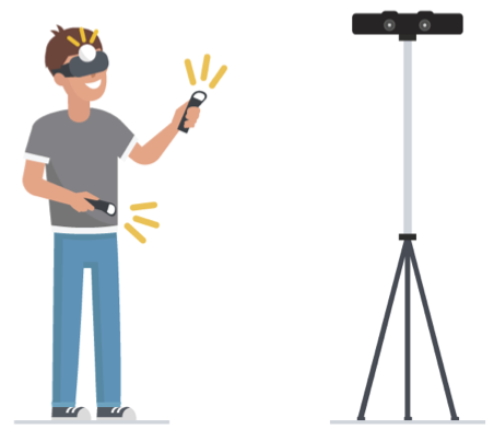
Figure 4. “Outside-in” positional tracking using stereo camera (placed in the room) to track user’s body motions and hand movements via LED markers mounted on headset and hand controllers.
In “inside-out” positional tracking a stereo camera mounted on the user’s headset (looking inside-out from user’s vantage point toward the room environment) is used to track user’s hand movements via LED markers mounted on hand controllers, as shown in Figure 5. The FPGA, located inside the head mounted camera unit, uses the stereo camera data to calculate user’s hand movements, which is then passed on to the mobile AP to be incorporated into the AR/VR application.

Figure 5. “Inside-out” positional tracking using stereo camera (mounted on user’s headset) to track user’s hand movements via LED markers mounted on hand controllers.
While both “outside-in” and “inside-out” systems provide an immersive experience, “outside-in” can provide a higher level of immersion since it can also track body motions (such are walking, running, squatting, jumping, etc.) using the LED marker on headset, there by transposing body motions in the real world into the virtual world.
In both systems, the user movements need to instantly appear in the virtual world with extremely low latency, in order for it to convey a “real” user-experience. ECP5 FPGA’s parallel processing capability is key to achieving this low latency. Additionally, it’s low power and small-form-factor packages are key to making this a mobile untethered experience.
Co-Processing and Bridging in Automotive ADAS
The automotive market is seeing a significant jump in demand for vision processing and connectivity solutions. Driven by new regulations requiring rear cameras in new automotive designs, as well as the introduction of cameras to replace side mirrors, offer blind-spot detection and lane tracking, analysts at market research firm IC Insights project the worldwide market for CMOS image sensors, led by new applications in the automotive sector, will grow at a CAGR of 55 percent between 2015 and 2020.
In this rapidly growing market, automotive designers will need solutions that can not only perform pre- and post-processing, but can also be used to build optimized connectivity solutions for Advanced Driver Assistance Systems (ADAS) and infotainment applications. As auto manufacturers develop more sophisticated ADAS systems, designers face two challenges. First, what is the best way to interface to the rising number of cameras? Most modern processors feature only two camera interfaces, while many ADAS systems require as many as eight cameras to meet rising autonomous feature requirements. Second, how do designers perform image processing on the rapidly growing amount of data coming from those camera sensors?
To address these challenges, they need a solution that will give them the co-processing resources to stitch together multiple video streams from multiple cameras or perform image processing functions (such as white balance, fish-eye correction, defogging) on the inputs from multiple cameras, and then pass that data on to the AP in a single stream. Auto designers also need the flexibility to drive multiple displays for dashboard, instrument clusters and rear-seat entertainment applications, and the ability to bridge between older legacy interfaces and new MIPI interfaces.
For many of these applications Lattice’s ECP5 FPGAs with automotive-grade (AEC-Q100) support can deliver the parallel processing capabilities required to accelerate the image processing pipeline, while the large number of I/Os can interface to larger arrays of cameras. An excellent example of this trend is the bird’s-eye view capability now available in many cars. Typically, this bird’s-eye view feature offers live video from 20 feet above the car looking down. The ADAS system achieves this by stitching together data from four or more cameras with a wide field-of-view (FoV).
Historically, designers have used a single processor to process image from a single camera. Today, designers can use a single ECP5 FPGA to replace multiple processors, aggregate data from multiple cameras, stitch the images together, remove fish eye, perform white balance, maximize image quality using HDR, and send a good quality image to the processor. Ultimately, designers using this approach gain better performance while driving down cost and power.
Figure 6 shows how one Lattice customer built such a solution. This bird’s-eye view system collects video from cameras located around the car (front, back and sides). An ECP5 FPGA processes and stitches together the video data to provide a spatial 360-degree view. In this case a single FPGA replaced multiple ARM processors. The final product is a crisp 1080p, 60 fps image. Aside from the ECP5, the board uses only a single low-end ARM processor to perform initial calibration and video encoding/recording.
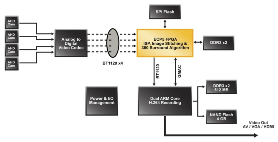
Figure 6. The diagram above illustrates how one developer used a single ECP5 FPGA to generate a bird’s eye view subsystem previously implemented using multiple ARM processors.
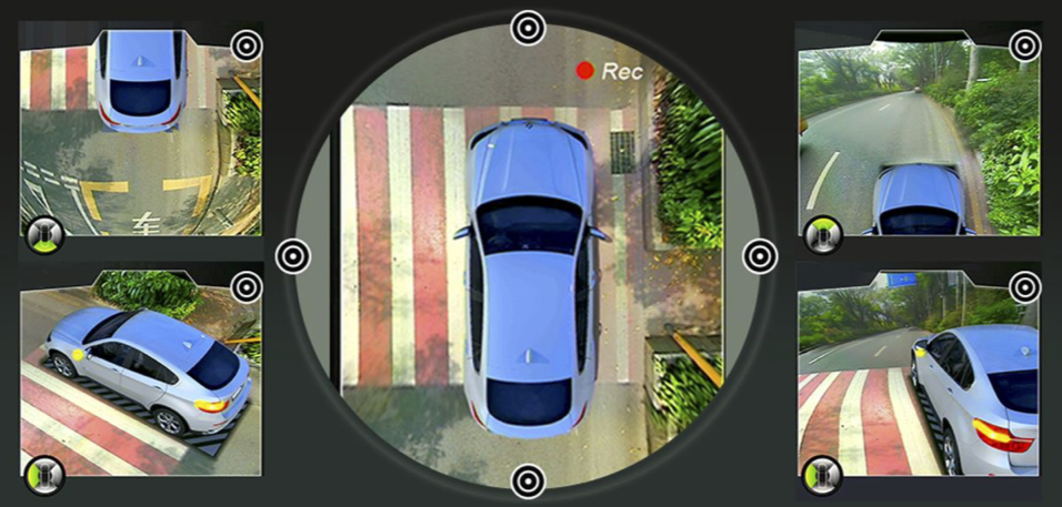
Figure 7. The figure above shows the resulting 360-degree view accomplished by a single ECP5 FPGA using inputs from four cameras.
Another key role FPGAs can play in automotive designs is serving as a cost-effective bridging solution between legacy interfaces and newer, increasingly popular MIPI cameras and displays.
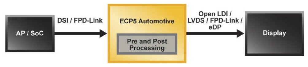
Figure 8. ECP5 FPGA in an automotive infotainment application performing both pre- and post-processing, and video bridging between the AP and displays.
In the Figure 8 block diagram, for example, ECP5 sits between the AP or SoC and one or more automotive displays, which allows it to perform both pre- and post-processing functions, and supports video bridging between the AP’s DSI or FPD-Link interfaces and displays featuring Open LDI, LVDS, FPD-Link or eDP interfaces. The FPGA can be used in a variety of other infotainment use cases as well, including splitting a single video output for dual rear-seat displays, and cropping and formatting video for a specific video resolution.
The significant processing resources on the ECP5 also open the door to a variety of sensor bridging, aggregation and co-processing applications. In Figure 9, ECP5 serves as an intelligent hub for control and aggregation of data from multiple types of sensors. By providing pre- and post-processing on the sensor data as well as I2C management functions and a SPI interface, the FPGA can dramatically reduce the computational load on the AP.

Figure 9. ECP5 FPGA acting as a data bridge and intelligent hub, controlling and aggregating multiple types of sensors.
Another bridging, aggregation and co-processing example utilizes the automotive-grade FPGA’s 3.2 Gbps SERDES capability to aggregate data from multiple RADAR or camera sensors and transmit it over in-vehicle networks like BroadR-Reach or Ethernet. In Figure 10, data from multiple sensors come into ECP5 via LVDS interface, where it gets aggregated and packetized, and is transmitted via SERDES-based SGMII interface to in-vehicle network.
Figure 10. ECP5 automotive-grade FPGA’s LVDS and 3.2 Gbps SERDES capability is used to bridge and aggregate data from multiple RADAR or camera sensors and transmit over SGMII to in-vehicle networks.
Machine Learning at the Edge
Looking ahead, interest is building for mobile-influenced solutions that leverage the application support and manufacturing scale associated with mobile processors and MIPI-compliant sensors and displays to enable intelligence at the edge. The demand is growing for solutions that employ Artificial Intelligence (AI), neural networks and machine learning to achieve that goal.
A neural network used in machine learning to perform image recognition is taught to recognize a cat, for example, by exposing it to thousands of images and assigning weights to the input until the network can correctly identify the image of a cat. Developing the data structure and assigning the weights can require terabytes of data and exaflops of computational power. Accordingly, the training aspect of machine learning using deep learning techniques typically occurs in the data center using high- end GPUs & FPGAs – which are needed to meet those gigantic computational requirements.
Once the model is trained, it is ported to embedded systems in edge applications to perform inferencing in applications such as image recognition or speech recognition. At the network edge, devices must make decisions more quickly and more efficiently from a computational standpoint. So, designers use inferencing techniques that take the lessons the network has learned during the ‘training’ phase and applying them to new data to ‘infer’ a result. For inferencing at the network edge, designers need solutions that offer a computationally-efficient platform and still meet stringent power, size and cost constraints.
There is widespread recognition in both industry and academia today that machine learning requires highly specialized hardware acceleration. But the requirements differ depending upon the task. For example, training and inferencing may require different hardware. Designers of hardware for training applications typically focus on computation with very high levels of accuracy often using 32-bit floating point operations. Designers of hardware at the network edge using inferencing, on the other hand, need the flexibility to sacrifice precision for greater processing speed or lower power consumption. In fact, recent research indicates that for many applications fixed-point computations deliver nearly identical inference accuracy compared to floating-point solutions while consuming less power.
With its extensive embedded DSP resources, a parallel-processing architecture that’s inherent to FPGAs, and a significant competitive advantage in terms of power, footprint and cost, the ECP5 FPGAs meet many of the requirements of this emerging AI market. The ECP5’s DSPs, for example, can compute fixed-point math at less power/MHz than GPUs using floating-point math. These characteristics offer an attractive advantage to developers of power-limited intelligent solutions at the Edge. Figure 11 shows an example where ECP5 acts as an inferencing accelerator running a pre-trained Convolutional Neural Net (CNN) function on data coming from camera sensors. CNN engine running on the FPGA recognizes objects or faces and passes on the results to system CPU, thereby achieving fast and low-power object / face recognition.
Figure 11. ECP5 FPGA acting as a Convolutional Neural Net (CNN) accelerator for object / face recognition in an intelligent edge application.
To expand on this further, the block diagram in Figure 12 shows neural net acceleration demo that performs face tracking in real-time and consumes only 0.85 W of total power on an ECP5-85 FPGA with 85K LUTs.
Figure 12. Real-time images captured by camera are input into the FPGA, which identifies faces and outputs an image with highlighted faces onto a display.
Implementing design in an FPGA gives designers the flexibility to scale it up or down to meet specific power vs. performance trade-offs required by the end system. In the above example, the design can achieve even lower power and fit into a smaller than 85K LUTs FPGA by trading off performance and other parameters – such as reducing frame rates, reducing frame size of the input image, or reducing number of bits used to represent the neural net weights and activations.
Moreover, the FPGA’s reprogrammable characteristics allow designers to meet market’s rapidly changing requirements. With FPGAs, as algorithms evolve, users can easily and quickly update their hardware via software. That is a capability GPUs or ASICs can’t match.
The above demo was developed on the Embedded Vision Development Kit (Figure 13), part of Lattice’s embedded vision solutions portfolio, which provides a modular platform for the development of embedded vision solutions for applications at the edge.
Figure 13. Lattice’s Embedded Vision Development Kit featuring ECP5 FPGA, CrossLink FPGA and HDMI ASSP.
Conclusion
Today’s designers are constantly looking for new ways to reduce cost, power and footprint, while adding more intelligent processing in their edge applications. At the same time, they must constantly keep pace with the rapidly changing performance and interface requirements of a new generation of sensors and displays used in edge applications. Lattice’s ECP5 FPGA family offer designers the best of both worlds. By delivering a high level of processing capability (with up to 85K LUTs) in the industry’s smallest package (10×10 mm) with SERDES, ECP5 FPGAs gives designers the co- processing and connectivity resources they require. And by offering those capabilities at lower cost and power than the competition, ECP5 gives developers the edge they need.