The device performs to a high standard with a total build cost of less than €5,000 and a development time of less than three months. This is largely due to the ease of hardware integration provided by LabVIEW and also the advanced and high-speed data processing capabilities that LabVIEW and NI vision provide.
– David Moore, Dublin City University
The Challenge
Designing and building a 3D optical surface profilometer capable of surface visualisation and roughness analysis to use in laser-processed surface characterization.
The Solution
Using NI LabVIEW software with the NI Vision Development Module to image acquisition, motion control, and raw data processing, as well as to provide a full-colour 3D surface display with surface profile and surface roughness analysis.
In the photovoltaic field, laser micromachining is often performed during the various manufacturing stages. However, these laser processes may involve ablation and melting, which can result in rough surfaces on specimens due to debris from the machining. It is often necessary to characterise the specimen surface condition and profile to evaluate the laser process performance. Optical profilometry techniques are preferred where possible as they do not interfere with the specimen surface and can measure large areas at a high resolution. However, optical techniques such as interferometry can result in difficulties in measuring rough and transparent specimens. By varying the focal plane of a specially designed optical and imaging system with a low depth of field, it is possible to extract surface contour information from the specimen. Advantages of this method include high resolution and surface visualisation in real colour.
Because the system contains components of motion control, image processing, surface display, and signal analysis, LabVIEW was an obvious choice as the software development environment due to its seamless integration with third-party hardware and other NI products such as NI Vision.
High-Resolution Optical and Imaging Systems
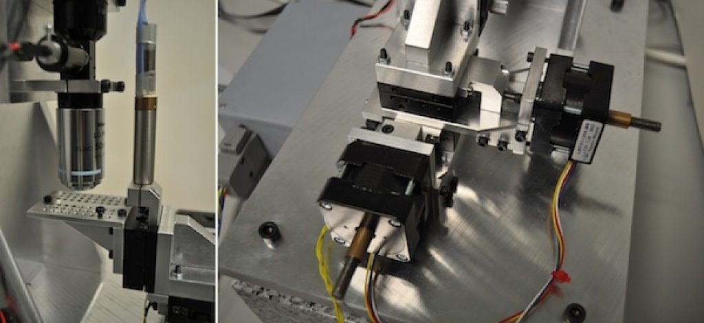
We implemented a high-resolution optical system using a 50X magnification Nikon microscope objective lens. This objective lens has the power to resolve features in the order of 500 nm using white light illumination and provides a very shallow depth of field, meaning only a fraction of the image is focused at any one time. We used this lens in conjunction with a microscope tube and a 3 MP colour USB camera as the imaging device. This configuration gives the optical system an overall magnification of 25X with a field of view of 240 by 200 µm.
Motion Control and Image Acquisition Synchronisation
There are two parts to the motion control system. The high-accuracy vertical positioning system positions the sample along the vertical axis of the optical system, thus changing the position of the focused optical plane. The high-accuracy Thorlabs servo actuator used for the vertical positioning of the specimen is controlled using a Precision Micro Control servo motor driver/amplifier, which is supplied with LabVIEW VIs.
Third-party hardware integration is seamless and simple because LabVIEW supports many third-party hardware components. This high-accuracy positioning system has a theoretical resolution of 40 nm. We controlled the XY positioning system with two Nanotec stepper motors using third-party USB stepper drivers. This provides5 µm resolution when full stepping, so the specimen can be accurately positioned and the mosaic acquisition can be implemented with image stitching for large area measurement. The USB stepper drivers also provide digital I/O ports which are used as camera triggers in conjunction with sequences in the software developed with LabVIEW to synchronise the vertical specimen position with the image acquisition.
Raw Image Data Processing
We then processed the raw data acquired in the form of a stack of images to extract the focus regions from each image in the stack. As the vertical position of each image is known from the synchronisation of the motion control system during the image acquisition, it is possible to build a 3D surface mesh from the extracted focused regions. We used a Sobel edge detection VI in NI Vision to perform the feature extraction. Using a Sobel edge detector, we can assign an intensity for the gradient of every pixel in the image being analysed. We then parse the stack of images to find the highest gradient intensity for each pixel along the vertical measurement plane. Then we reference the highest intensity to a height according to the vertical position that image was recorded at, which is stored in a ‘height map’.
3D Surface Visualisation
We can then visualise the 3D surface in full colour using software created in LabVIEW. We used a built-in LabVIEW VI to process the height map of the surface, which is then ready for display in a 3D picture control. Using a 3D picture control configuration VI, we can wrap the fully focused image (previously generated from the stack of images by extracting the focused regions) on the surface mesh to display the measured specimen in full colour at submicron resolution.
Surface Roughness Analysis
We must often measure the surface roughness of components in surface engineering. Different surface roughness parameters reveal different important characteristics of the material and the production processes. However, there are strict guidelines that we must meet to make roughness analysis repeatable and accurate. First, the data must be corrected for form error by linear regression. This step involves using a Gaussian filter with a low cut-off frequency defined by ISO 4288, which removes the waviness component of the surface. The waviness may appear as a repeating pattern in the data when the wavelength is too large to be considered as roughness. We use the remaining for the roughness analysis. We can perform two types of analysis using this software; line analysis and area analysis, where the area analysis provides similar information to that of the line analysis but in two directions instead of one.
While the actual resolution of the measurement depends somewhat on the specimen being measured, it is certain that measurements are accurate in the submicron range in the X, Y, and Z planes. Measurement speed also reflects the high performance provided by the LabVIEW environment. It is possible to perform a single measurement of an area of 240 by 200 µm with submicron resolution in less than 60 seconds including data processing and surface visualisation, using only a standard dual-core PC. The device can also perform large surface area measurements up to a maximum of 20 by 20 mm and can measure rough sample surfaces, a difficult task using other optical profilometry techniques.
Author Information
David Moore
Dublin City University