
This technical article was originally published on The Linley Group website on behalf of Coherent Logix. It is reprinted here with the permission of The Linley Group and Coherent Logix.
After spending 15 years targeting military/aerospace, software-defined radios (SDRs), and other niche applications, Coherent Logix is expanding into the commercial edge-AI market. Customers have deployed its previous-generation software-configurable embedded processors— called HyperX—in 3G/4G small cells, GPS receivers, radars, sensor processing, and video analytics. In addition to handling general-purpose and signal-processing workloads as well as neural-network inference, the processor is well suited to cybersecurity and video transcoding.
Coherent describes HyperX as a memory-network technology, owing to its array of processor elements (PEs) that connect through a programmable mesh of data-memory routers (DMRs). Customers can use the chip to implement multiple independent heterogeneous function blocks, as Figure 1 shows. The function-block configurations and resource assignments are run-time programmable, as are the core voltages and clock frequencies.
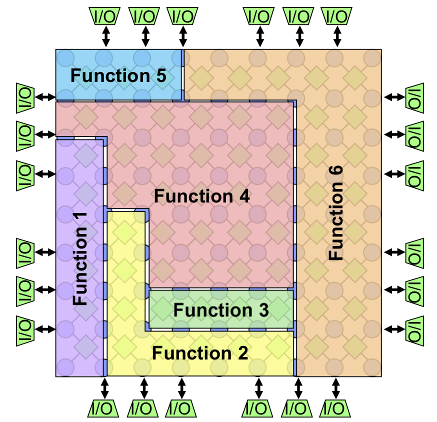
Figure 1. HyperX memory-network processor. The architecture combines an array of processor elements (PEs) interleaved in an array of data-memory routers (DMRs). Customers can configure a variety of AI, computer-vision, DSP, and general-purpose functions by defining compute and communications tasks that execute concurrently.
For DSP workloads, HyperX offers configurability similar to an FPGA’s, allowing designers to implement various parallel or serial algorithms. But unlike an FPGA, it’s programmable without using RTL, it requires no place-and-route software to create the physical layout, and it avoids the iterations typically necessary to achieve timing closure. Without changing any software, developers can make power and performance tradeoffs by simply changing the compiler constraints, forcing all or part of an application to run in parallel or serially across the available resources.
Coherent plans to offer a range of devices in its new HX4-series lineup, but it first developed the HX40048 for an undisclosed customer. It’s using the HX40048 test results to develop the HX40416, which it plans to tape out by year-end. Packaged HX40416 chips and development boards are scheduled to sample in 3Q21. GlobalFoundries manufactures these latest processors in its 14nm FinFET technology.
The last four digits in the HyperX part numbers represent the chip’s PE count. The HX40416 places 416 PEs in a 16×26 matrix overlaid by a 17×27 array of DMRs (459 total DMRs). Additionally, it integrates a SiFive U54 CPU capable of running Linux and other high-level operating systems, but that CPU is unnecessary for the chip’s operations. The PEs support a total of 1,664 INT16 MAC operations per cycle, equivalent to 6.6 trillion operations per second (TOPS) at the 2.0GHz maximum clock rate.
A Software-Defined Architecture
Coherent Logix began as a subsidiary of SPEC, which for more than 30 years has launched a variety of businesses to work on government-funded R&D projects. In 2005, Coherent became an independent company supported by a series of Small Business Innovation Research (SBIR) grants from Darpa, NASA, and the US military. Its projects included software-defined antijamming GPS, radar, and remote-sensor radios. In 2009, the company’s earlier-generation HyperX processors flew to the International Space Station.
After a small initial investment, Coherent has funded its growth from profits. Most of its 70 employees work at its Austin headquarters and other engineering offices in the US and Canada. CEO and CTO Michael Doerr founded the company after previously serving as managing director of SPEC’s SoC-products division. In the same year that it became independent, Coherent developed the first-generation HyperX, which it delivered to a diverse group of customers including BAE Systems, Dolby, L3com, LG, and Rockwell Collins. Two years later, its second-generation product enabled software-defined GPS and video analytics. In 2013, its third-generation 65nm offering won designs in ATSC 3.0 broadcasting, genome mapping, SSDs, and other devices.
Each HyperX PE is an independent SIMD/VLIW DSP engine that’s 64 bits wide and C programmable, running at up to 2.0GHz in the 14nm models. The PEs employ tightly coupled memory in the four adjacent DMRs. The architecture supports an event-driven data-flow model in which the cores conserve power by turning off their clocks until the required data and instructions become available.
The PEs execute scalar and vector operations using INT8, INT16, INT32, and single-precision floating-point (FP32) operands. On each clock cycle, a core can execute up to four 16-bit compute instructions, a single FP32 operation, or other scalar and vector operations such as address generation, shifts, and zero-overhead loops. Customers can scale performance by cascading multiple chips connected directly to the edge I/Os. The HX40416 model will integrate a DDR DRAM interface, but Coherent also plans to allow buyers to customize their devices using chiplets, including CAN, Ethernet, HDMI, PCIe, USB, and other standard I/Os.
Neighborly Relations
As Figure 2 shows, the HyperX DMRs have eight configurable communication ports, which in addition to the PE connections include four links to other DMRs in the north, south, east, and west directions. Each port comprises 4×16-bit channels that support simultaneous communications in all eight directions. PEs can concurrently execute two 64-bit reads and one 64-bit write per clock, and they can concurrently execute instructions from one memory block while loading new instructions into a second memory block. If a PE needs more storage for a particular function, the program can extend its memory space by defining additional DMR overlays.
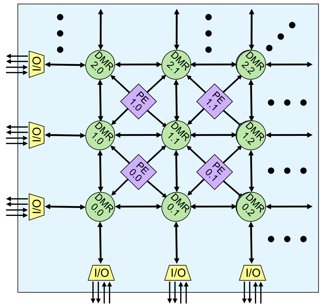
Figure 2. HyperX architecture. DMRs connect with adjacent DMRs and PEs through 64-bit communication links containing four independent 16-bit channels. A separate messaging fabric, not shown in the figure, allows processor reconfiguration at boot time or run time. In the HX40416, the DMRs and PEs operate at the same 2GHz maximum clock rate.
Despite their name, the DMRs store instructions as well as data. In the HX40416, each one integrates a 48KB SRAM organized as 8Kx16-bit instruction words and 16Kx16-bit data storage. The total on-chip storage is 20MB. A separate message fabric (not shown in the figure) allows dynamic processor reconfiguration by loading new instructions from external memory. The DMRs offer a pass-through mode, which lets data move across the fabric from source to destination without employing the intermediate DMR resources.
Developers describe their application and its parallelism using C/C++ and the industry-standard message-passing interface (MPI). The compiler maps the compute tasks and required communications to the physical hardware. Compute tasks execute in the PE’s ALUs, and communication tasks execute autonomously and concurrently in the DMRs. Data hops from one DMR to the next in one clock cycle and there are no caches, so the processor’s execution is deterministic. At the fabric edge, DMRs treat off-chip I/Os as another node, allowing data to feed directly into and out of the fabric. The I/Os can extend the mesh by connecting directly to another HyperX chip, to external memory, or to other customer-defined interfaces.
The programmable-mesh architecture gives developers the flexibility to optimize mapping of neural-network models and other functions to the available compute and memory resources. The HyperX communication channels and PEs are configurable to implement data parallelism, task parallelism, pipelined operations, or a combination of these control-flow models. Unlike deep-learning accelerators (DLAs) that employ fixed hardware blocks, such as systolic MAC arrays, HyperX can achieve high utilization by fitting the hardware to the algorithm. In an example ResNet-50 network using a batch size of one, it achieved 70% average utilization.
To accommodate variable tensor dimensions, developers can also implement a variety of multidimensional memory structures throughout the chip. The mesh communication channels are run-time configurable to support one-to-one, one-to-many, many-to-many, or any combination of these communication modes. The ability to broadcast data is useful for computer vision, in which different neural-network nodes operate on different portions of a feature map. A many-to-one structure is ideal for pooling layers.
Balancing Performance and Power
Before committing an application to a particular configuration, designers can tune its performance using Coherent’s cycle-accurate simulator. The Eclipse-based integrated software-development environment (HXISDE) allows mapping of applications to the chip’s resources in multiple ways, depending on the performance/power requirements.
The HXISDE lets developers visualize applications based on modular programming techniques as a hierarchical assembly of functions—“cells” in the company’s lingo. Higher-level functions combine multiple cells, which connect to each other by declaring the input and output ports. Programmers archive these functions into a library for their application, but because all the HyperX processors are code compatible, the functions are reusable on other devices.
Figure 3 shows an example of the area, performance, and power tradeoffs for an object-detection neural network in the HX40048. The three curves represent power and throughput scaling across a range of clock frequencies and number of PEs employed. In this example, after compiling the network using the same number of PEs for every layer, the developer evaluated the various operating points without changing the software to alter the parallelization. Running at 1.5GHz, image throughput doubles from 2 to 4 cores per layer and then falls off to an 80% increase from 4 to 8 cores and about a 70% increase from 8 to 16.
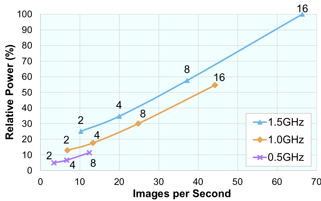
Figure 3. HyperX HX40048 performance/power scaling. In this example, implementing a neural network using eight cores per layer running at 1.0GHz delivers 25% greater throughput than four cores running at 1.5GHz, but the larger design consumes 15% less power. (Source: Coherent)
The curves also show the impact of voltage/frequency scaling. A four-core design using the low-power 0.5GHz operating point delivers the same throughput as a two-core design running at 1.0GHz, and it consumes half the power. The tradeoff is that it needs twice the resources. In an alternate configuration, designers can duplicate cells to process multiple images concurrently. The additional parallelism achieves linear scaling, albeit at the expense of greater area and power.
The company supports HyperX with a software library that includes prebuilt functions for computer vision, deep learning, image processing, video encoding, and wireless communications. The neural-network design flow handles models developed in the Caffe and TensorFlow frameworks. The deep-learning library comprises functions for common convolutional-neural-network (CNN) layers such as matrix multiplication, ReLU activations, and softmax pooling, as well as functions for pruned and sparse layers. The SDK also has tools that allow programmers to convert Python programs with OpenCV graph-API calls into a computational graph based on HyperX library functions.
A Versatile Edge Processor
Coherent’s HyperX design has several features like those of Blaize’s El Cano processor (see MPR 9/7/20, “Blaize Ignites Edge-AI Performance”). Both edge-AI chips implement a data-flow architecture that supports data, instruction, and task parallelism. Each also optimizes efficiency by exploiting data dependencies in computational graphs.
Whereas El Cano’s graph-streaming-processor (GSP) cores include special-function units that handle DSP operations, along with multiprocessing SIMD units for neural-network acceleration, HyperX PEs are more-powerful VLIW DSPs originally designed for software-defined radios and video analytics. The HX40416 employs a deterministic memory-network architecture, which contrasts with the much smaller multilevel cache system and dynamic thread scheduler that control El Cano. Because it has 16-bit MAC units, however, the HX40416 delivers less than half of El Cano’s throughput on the INT8 operations common to inference workloads.
Like HyperX, Hailo’s Hailo-8 processor also configures its compute, control, and memory units to separately handle each neural-network layer (see MPR 6/24/19, “Hailo Illuminates Low-Power AI Chip”). But its PEs only execute neural-network operations and aren’t designed for general-purpose or DSP functions. Nevertheless, Hailo-8 can deliver four times as many TOPS as the 16-bit MAC units in the HX40416, and it integrates a much larger SRAM capable of storing more network parameters on chip, as Table 1 shows.
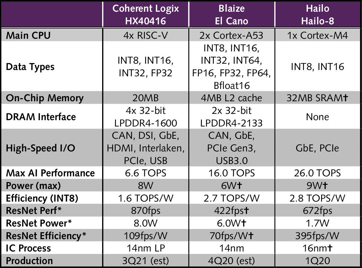
Table 1. Comparison of edge-AI processors. The Blaize and Coherent chips provide similar programmability, but the HX40416 is better suited to DSP and general-purpose computing as well as neural-network inference. *ResNet-50, batch=1. (Source: vendors, except †The Linley Group estimate)
Running ResNet-50 on its 16-bit MAC units, the HX40416 can deliver 870fps, according to the company’s projections of the HX40048’s performance. That number represents 30% greater performance than Hailo-8’s 8-bit MAC units can provide, but whereas HyperX uses all of its resources to deliver that peak throughput, Hailo-8 uses just a fraction, resulting in one-fifth the power consumption.
HyperX customers have the option to reduce power by employing voltage/frequency scaling or by configuring the network with fewer PEs and DMRs. But at the same throughput as Hailo-8, we believe the HX40416 will still consume more power. Although the Hailo chip is unlikely to achieve close to 100% utilization, its 26-TOPS maximum throughput allows it to offer additional resources for more-complex networks than the HX40416 can run.
Blaize hasn’t published ResNet-50 performance, but on the basis of El Cano’s 50fps Yolo v3 performance, we estimate it can deliver 422fps on the less complex network— about half of the HX40416’s throughput. Its power efficiency is approximately 35% less than HyperX’s and only 18% of Hailo-8’s.
The HX40416’s greatest advantage over these competitors is versatility. Users can program El Cano to execute other computational-graph types, but that capability supports portions of the computer-vision pipeline, such as the ISP, rather than general-purpose and DSP functions. Likewise, Hailo-8 is a purpose-built computer-vision processor. HyperX can handle those functions as well as a variety of edge-computing tasks.
Go to Commercial
After 15 years in business, Coherent Logix is no longer a startup, but its shift to commercial devices is equivalent to a new venture. Its competitors have keenly focused on developing edge-AI processors from the outset, whereas Coherent is adapting an architecture initially developed for specialized DSP workloads. Inference processors rarely need HyperX’s floating-point capabilities, and 16-bit integer precision is overkill for most AI applications. The company designed another HX40416 configuration that can deliver twice the throughput for INT8 MAC operations, but the initial model runs them at the same rate on the 16-bit MAC units.
Nevertheless, HyperX offers the flexibility to handle a variety of workloads—an advantage for many systems. For example, in the company’s demonstration of an Ethernet-connected computer-vision system, the HyperX chip does packet processing, image preprocessing, feature detection, and keypoint filtering, producing an output to the Ethernet interface that comprises bounding boxes and object descriptors. Customers evaluating HyperX for such applications should compare total system cost and power consumption with those of the alternative multichip solutions.
By packaging its device using chiplets tailored to each customer, Coherent’s go-to-market strategy is akin to an ASIC provider’s rather than a processor vendor’s. The finished-product cost will be about the same, but a software-configurable HyperX processor reduces development time and supports field upgrades. HyperX gives developers more options to control performance and power, including at run time, yielding an advantage over other programmable-logic chips.
The company has grown its business organically, but producing a 14nm chip is much more expensive than its earlier projects. In comparison, the third-generation processors it unveiled in 2013 use a low-cost 65nm technology. Coherent compares the HX40416 with Hailo-8, Intel’s Myriad, and Nvidia’s Jetson, but the HyperX chip is a better fit for those needing a custom solution for low-volume applications. HyperX is a flexible power-efficient architecture, but to address the same high-volume markets as the competing products, Coherent will need additional funding to develop a complete SoC.
Price and Availability
Coherent Logix withheld target pricing for its next-generation HyperX processors. It plans to tape out the HX40416 by year-end, with production planned for 3Q21. More information is at www.coherentlogix.com.
Mike Demler
Senior Analyst, The Linley Group