This blog post was originally published at Lattice Semiconductor’s website. It is reprinted here with the permission of Lattice Semiconductor.
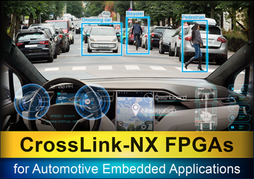
Countries around the world are mandating that vehicle manufacturers install various advanced driver-assistance systems (ADAS) capabilities and functions. These ADAS features demand sophisticated detection capabilities using a combination of sensors, including image (camera), LiDAR, radar, ultrasonic, and far infrared (FIR) devices. In fact, according to industry analyst firm P&S Intelligence, “…the global advanced driver-assistance system (ADAS) sensor market is expected to reach $40.8 billion by 2030, advancing with a CAGR of 11.7% during 2020–2030…”
Consider the following image of what would currently be considered a relatively typical automobile, in which each sector represents the area being observed by a different sensor for use with ADAS applications.
A typical complement of automotive sensors used for ADAS applications.

The cameras capture high-fidelity images of the road and surrounding environment to be interpreted by on-board computers, but these images are limited to what the cameras can “see” in the visible spectrum. Also, the quality of camera images can be degraded by environmental conditions like fog and rain. The radar and ultrasonic devices generate radio and audio frequency pulses and capture the responses that bounce off objects. These sensors work in all weather conditions but cannot be used to differentiate between different types of objects. Similarly, LiDAR devices generate pulses of light and capture the responses that bounce off objects. In addition to observing road features like lane markings, LiDAR sensors — which operate in both light and dark conditions — can also be used to detect animals, pedestrians, and other vehicles. Meanwhile, FIR thermal sensors capture the IR radiation emitted by objects, work in the dark, and can be used to differentiate between animate and inanimate objects. Signals from all of these sensors have to be processed. In many cases, representations of the sensor data are then required to be displayed to the driver on one or more in-cabin displays.
In many cases, the information derived from multiple sensors needs to be merged in a process known as sensor fusion. Increasingly, in-cabin applications (e.g., gesture recognition), ADAS applications, and in-vehicle infotainment (IVI) applications (e.g., e-mirror, rearview/backup) require some amount of artificial intelligence (AI) and machine learning (ML). In fact, it is forecast that AI will be employed in the majority of ADAS and IVI systems by as soon as 2025. This presents automotive system designers with a challenge as supporting multiple sensors and processing the data they generate requires an expensive application processor (AP) with multiple I/Os and significant processing capabilities. To help lower the overall cost of an ADAS system, designers should consider an alternative to the costly CPUs and GPUs that typically serve as the hardware platform in an ADAS system. One such alternative is to use a less robust AP (with fewer I/Os and lower processing power to keep costs down) in conjunction with a low-power embedded vision IC like the Lattice CrossLink™-NX FPGA.
In such a solution, much of the sensor data is pre-processed by the FPGA so the AP can focus its processing resources on enabling the ADAS system’s AI functionality. The CrossLink-NX FPGA can combine the various sensor data streams and forward them on to the AP using a process called sensor aggregation to reduce the number of I/Os the AP must support. In other cases, such as taking a video signal and using it to drive multiple displays, the CrossLink-NX can replicate the video stream using a process called display splitting. Additionally, when it comes to safety-critical systems that require redundant data, the data from one or more sensors may be replicated and sent to multiple APs from a single CrossLink-NX FPGA.
Developers may question what impact adding another IC to their design could have on power and design footprint constraints. They needn’t be concerned as CrossLink-NX FPGAs, which are built on the Lattice Nexus™ FPGA development platform, consume up to 75 percent lower power vs. similar competing FPGAs and are available in small form factor packages as small as 6 mm x 6 mm. And with support for a cornucopia of high-speed interfaces, including two dedicated 4-lane MIPI D-PHY transceivers running at 10 Gbps per PHY, CrossLink-NX FPGAs provide best-in-class performance for vision processing, sensor processing, and AI inferencing applications.
CrossLink-NX FPGAs also offer a Soft Error Rate (SER) up to 100 times lower than similar FPGAs in their class, which makes them a compelling choice for mission critical applications like ADAS that must operate safely and reliably. The really exciting news is that the CrossLink-NX FPGAs are now AEC-Q100 qualified up to Grade 2 (TA = 105°C), which makes them ideal for automotive applications.
Finally, CrossLink-NX FPGAs are fully supported by the Lattice mVision™ and sensAI™ solution stacks. These solution stacks significantly reduce the time and engineering expertise needed to implement automotive embedded vision applications by providing developers with modular hardware platforms, reference designs, neural network IP cores, and custom design services to accelerate and simplify automotive vision system design.
Automotive applications enabled by the mVision and sensAI solution stacks.

The Lattice mVision solutions stack includes everything embedded vision system designers need to evaluate, develop, and deploy FPGA-based embedded vision applications, such as machine vision, robotics, ADAS, video surveillance, and drones. Meanwhile, the full-featured Lattice sensAI solution stack includes everything required to evaluate, develop, and deploy FPGA-based AI/ML applications.
In summary, Lattice’s value proposition for automotive applications using AEC-Q100 qualified CrossLink-NX FPGAs includes low power (they boast high thermal margins with their 28 nm process), high reliability (best-in-class), high performance (10G MIPI, SERDES, and best-in-class I/O), small size (resulting in board real estate savings without compromising performance), high security (they meet ISO 21434 guidelines and NIST SP 800-193 compliance), high functional safety (they boast a planned ISO 26262 FuSa-compliant FPGA tool chain for safety-critical applications), and cost-feature benefit. We truly do live in a golden age for automotive ADAS/IVI applications.
JP Singh
Automotive Segment Marketing Manager, Lattice Semiconductor