This market research report was originally published at the Yole Group’s website. It is reprinted here with the permission of the Yole Group.
Smartphone Application Procession Unit (APU) vendors earned $8.3B revenue in Q4-2022. Products like the Snapdragon 8 Generation 2 help Qualcomm maintain their leadership position in this APU market.
This full reverse costing study was conducted to provide insights regarding the technology data, manufacturing cost, and selling price of the Qualcomm Snapdragon 8 Gen 2 system-on-chip (SoC).
One of the biggest chip manufacturers in the world, Qualcomm retains its leadership in smartphone SoC development. The Snapdragon mobile platform is one of their primary processor series that boosts the data processing and power management for high-end smartphones. The newest generation, Snapdragon 8 Gen 2, was released in late 2022. It is now used by several smartphone brands, such as Xiaomi, IQOO, Samsung, Vivo and Nubia Technology.
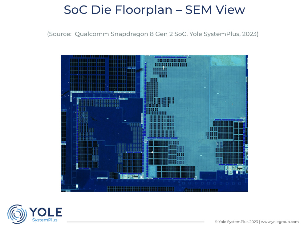
According to Qualcomm, the Snapdragon 8 Gen 2 SoC introduces a new powerful Central Processing Unit (CPU) with speeds up to 3.36 GHz. It has an Artificial Intelligence (AI) engine performing 4.35 times faster than its predecessor, an updated AdrenoTM Graphics Processing Unit (GPU), the latest Snapdragon X70 5G modem-radio frequency (RF) system and a FastConnect™ 7800 Mobile Connectivity System for WiFi 7 applications. The floorplan in this report reveals that the CPU is a new big-LITTLE architecture including the newest Arm Cortex-X3, Cortex-A715, A710 and A510 cores. The SoC die is manufactured using TSMC 4 nm lithographic technology instead of Samsung’s 4 nm process, which Qualcomm used for fabricating Snapdragon 8 Generation 1.
The package structure of Snapdragon 8 Gen 2 is similar to 8 Gen 1. The whole chip contains SRAM caches in the SoC die and includes an external LPDDR5X DRAM with packaging. Advanced ball-grid-array packaging technology is used for integrating the SoC die with upper and bottom substrates, then the DRAM package is stacked on the SoC die package with PoP (Package-on-Package) technology.
This report starts with the smartphone teardown on Xiaomi 13 to show how Snapdragon 8 Gen 2 and the components around it are integrated onto the main board of the phone. It provides multiple analyses from the Front-End-of-Line (FEOL), back-end construction to SoC assembly. We conducted detailed studies of chip packaging and SoC die cross-sections using optical microscopy, Scanning Electron Microscopy, material analyses and delayering.


We reveal the TSMC 4nm FinFET structure by high-resolution Transmission Electron Microscopy (TEM) analysis and then compare it with TSMC 5nm technology. In addition, Coherent Tomography 3D X-ray scanning shows the layout of the SoC die package. A floorplan study of SoC die offers a clear view of Intellectual Property (IP) design. Furthermore, we present a physical comparison of packaging, die manufacturing and floorplan between 8 Gen 2 and 8 Gen 1 SoC. Lastly, this report furnishes a complete cost analysis and a selling price estimation.