Semiconductor packaging can be incredibly boring. That said, advanced packaging is a key to every high-complexity semiconductor – both on and off the planet. Nvidia, AMD, and Intel have all utilized chiplets and advanced packages for their latest AI/ML accelerators and processors. Without 2.5D and 3D design and assembly techniques, these and many other essential products would not be feasible.
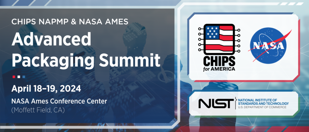
On April 18-19, 2024, the CHIPS R&D National Advanced Packaging Manufacturing Program (NAPMP) held an event focused on the critical role of advanced packaging in semiconductor manufacturing. This program originated from the CHIPS Act and has oversight from the US Department of Commerce.
The event highlighted the necessity of advanced packaging to achieve greater function, performance, and power savings than conventional chip packaging methods. Debates revolved around solving technological challenges associated with designing and assembling chips compactly that mimic a single traditional large chip. This debate addressed power supply, heat dissipation, testing, and repair complexities for tightly coupled assemblies.
The elephant in the room: Large companies have the resources to implement these advanced many-chiplet solutions. That leaves smaller innovative companies out in the cold.
What to do?
In almost every session, there was a desire to create a domestic, competitive, advanced packaging prototype and a low-volume production facility. It would open access to everyone, with a priority and cost structure appealing to innovative startups. The NAPMP aims to accelerate the transfer of packaging innovations into high-volume manufacturing, develop digital tools to reduce engineering costs, and establish facilities to pilot advanced packaging technologies. The program also seeks to train semiconductor personnel and students in relevant technologies to support domestic manufacturing facilities.
There are a lot of moving parts in this project. If one or two of them go wrong, the project could fail. Critically important: collaboration at levels unseen since Sematech in the 1980s. It may become more complex than Sematech, including the need to standardize processes and architectures across fabrication and assembly, with testing and yield management required at every step. Blurring the lines between fabrication and assembly – it will not be easy. A call for collaboration rang out between the CHIPS National Semiconductor Technology Center, the CHIPS Manufacturing USA Program, the CHIPS Metrology Program, and the US industry and academia to realize the vision of a robust domestic advanced packaging ecosystem. I sincerely hope that sufficient leadership emerges to drive the development of a next-generation development and early manufacturing facility.
The most critical challenges include:
- Design and Assembly: How to design and assemble chips so tightly that they behave like a single traditional large chip with the production efficiency and cost savings of advanced packaging.
- Power and Heat Management: Addressing the complexities of supplying power to and dissipating heat from tightly coupled assemblies.
- Testing and Repair: Developing methods to test and repair complex assemblies, especially when traditional visual inspection methods are not feasible due to small, tightly packaged dimensions.
- Reliability: Ensuring the reliability of advanced packaging, which is critical for the performance and longevity of semiconductor devices.
Take-Aways
Going in, it felt like a “we’re from the government, and we’re here to help” session. I gradually talked myself out of my skepticism and started feeling that a government-industry-academia collaboration could actually work.
What has changed to change my mind? Competition with China. With this as a motivator, I hope we can regain manufacturing leadership in semiconductors in the US. What do you believe?
George Jones
Managing Director, Woodside Capital Partners
Woodside Capital Partners is one of the leading corporate finance advisory firms for tech companies in M&A and financings in the $30M –$500M segment. The firm has worked with some of the best entrepreneurs and investors since 2001, providing ultra-personalized service to select clients. Our team has global vision and reach, and has completed hundreds of successful engagements. We have deep industry knowledge and extensive domain experience in the following sectors: Autonomous Vehicles and ADAS, Computer Vision, Artificial Intelligence, CloudTech, Enterprise Software, Information Security, Digital Entertainment & Lifestyle, Health Tech, Internet of Things, Networking / Infrastructure, Robotics, Semiconductors, Batteries, and Energy Storage. Woodside Capital Partners is a specialist in cross-border transactions, with extensive relationships among venture capitalists, private equity investors, and corporate executives from global 1000 companies. More about Woodside Capital Partners here.