AI data centers and cloud computing are demanding strong investment from countries all over the world. The word “Sovereign AI” has become popular with countries building out their own AI infrastructure, and AI data centers are now even being called “AI Factories.” With the rising prevalence of these data centers, the accelerated computing chips needed within them are hot in today’s markets. Namely, these are AI chips, such as advanced CPUs, GPUs, ASICs, and emerging AI chip technologies. IDTechEx‘s report, “AI Chips for Data Centers and Cloud 2025-2035: Technologies, Market, Forecasts” reveals current and emerging AI chips in the market, and their implications on the broader AI market.
The scale of GPU deployments
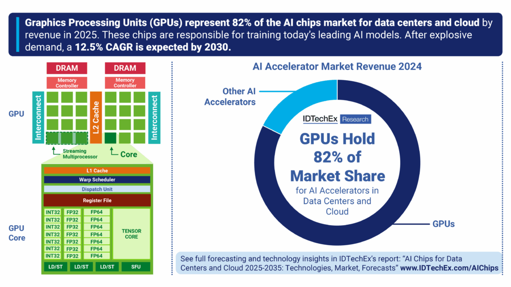
IDTechEx estimates GPUs (graphics processing units) drew 82% of the total AI chips revenue in 2024, and in 2025 the volume of GPU deployments is set to increase exponentially. This is largely led by tech giant, NVIDIA, which introduced its latest Blackwell GPUs in 2024, and has ramped up deployments throughout 2025. However, AMD is the current contender for data center GPUs with its MI300 and latest MI350 series, which are also winning major shipment deals for large scale GPU clusters. The major buyers continue to be the US hyperscalers AWS, Microsoft, Meta, and Oracle.
NVIDIA told investors in May 2025, that major hyperscalers are each deploying nearly 1,000 NVL72 racks (72,000) Blackwell GPUs per week, with conservative estimates reportedly looking at 2.5 million Blackwell GPUs (GB200) being shipped in 2025. AMD sees growing shipments of its MI350 series, with volume production beginning in June 2025. One of AMD’s largest deals is a multibillion-dollar collaboration with Humane to build AI infrastructure powered entirely on AMD CPUs, GPUs and software, as well as a deal with Oracle with up to 130,000 MI355X GPUs.
GPUs began as graphics processors, and are now the backbone for training AI
Graphics processing units (GPUs) have been used for graphics rendering and computingpower since the 1970s. IBM and Itari were some of the first chip designers, developing hardware for graphics in personal computers and arcade machines, which dealt with simple 2D rendering operations. The 1990s saw the next boom in technology, with 3D graphics gaining traction.
Moving into the 2000s, GPUs were used for scientific computations, like simulations and image processing, using software libraries created specifically to leverage parallel processing capabilities. This was adopted outside of academia when NVIDIA released CUDA and AMD released Stream SDK (now ROCm) in the late 2000s. This crucially allowed developers to use GPUs for general-purpose computing, instead of just graphics.
Interest in AI was popularized in the early 2010s with prominent AI models like AlexNet, ResNet, and Transformers all demonstrating deep learning and natural language processing capabilities. These models were optimized to work on NVIDIA GPUs and utilized NVIDIA’s libraries and frameworks. These models, using GPUs, set new benchmarks in performance across various AI tasks. GPUs are now used for their ability to perform massive parallelism, reach high data throughputs, and support advanced libraries (e.g., cuBLAS and cuDNN) that provide high-performance routines for linear algebra and deep learning. This is what is needed for training the largest of today’s AI models, including the likes of OpenAI’s ChatGPT, Anthropic’s Claude, or Google‘s Gemini.
The technology fundamentals of GPUs
GPUs, or graphics processing units, are made of thousands of cores that execute instructions in parallel. Every core is optimized for executing the same instruction across multiple data points simultaneously, which is known as SIMD (Single Instruction, Multiple Data). Each core is much simpler than those found in CPUs.
Compared to CPUs, GPUs have less advanced cache systems, however they have more transistors dedicated to computation, therefore they can sacrifice latency optimization in favor of high throughputs. This architecture allows GPUs to perform tasks requiring matrix multiplications and parallel compute at both faster throughputs, and greater efficiencies.
Each GPU core has capabilities for performing calculations in specific data formats with varying precisions (e.g. FP32 would be a high precision, and FP4 would be very low), which make them suitable for a range of AI workloads. In fact, these data center GPUs have specific cores called tensor cores, which are designed explicitly for matrix multiplications needed for neural network training and inference.
Lower-precision, mixed-precision, and specialized data formats are fundamental in high-end GPUs today. Low precisions especially allow for fast AI inference: NVIDIA already uses down to FP4, and AMD has announced FP4 compatibility with its MI355X processor.
For GPU designers, having software which can utilize these cores effectively is a key barrier, and is where market leaders have an advantage, especially with massive developer communities.
Key technology trends and challenges for data center GPUs
High-performance GPUs continue to adopt more advanced transistors, with 2nm, and 18A nodes being announced from 2026 onwards. These advanced nodes increase the performance of GPUs through increased transistor density. However, these advanced nodes will require High-NA EUV (extreme ultraviolet) lithography equipment from ASML, which will cost upwards of $780 million per machine.
Other challenges come from low yields, higher heat production, high R&D costs, and materials challenges. The economic value of pursuing smaller nodes is becoming less clear, and it is becoming harder to justify the investment.
Many players are instead increasing the total silicon area, which means increasing the number of transistors in a chip. Key technology strategies include stitching dies together (e.g., NVIDIA’s Blackwell GPUs and Cerebras’ non-GPU Wafer Scale Engine), and chiplet technology with 3D stacking (e.g., AMD’s MI300 and MI350 Series GPUs). Chiplets allow for higher yields, but can suffer from lower memory bandwidths.
Advanced packaging is critical. NVIDIA and AMD use 2.5D CoWoS packaging from TSMC. CoWoS packaging from TSMC has reached capacity, which may see companies using other foundries and similar technologies to match demand. AMD faces this issue, with ASE, Amkor, Powertech, and KYEC being potential partners for alternative advanced packaging techniques.
High-bandwidth memory (HBM) sees adoption across the board to deliver the memory needed for large AI models. HBM comes from three main players, Samsung, SK Hynix, and Micron, which are now seeing the adoption of HBM3e in top GPUs. Mass production of HBM4 is expected in 2025H2 (SK Hynix). Chinese players have also began domestic HBM production, such as Huawei, CXMT, Wuhan Xinxin, and Tongfu Microelectronics.

The AI chips market continues to evolve, and whilst GPUs remain the dominant technology, they do face challenges. Other AI chips include custom ASICs (application specific integrated circuits) developed by the hyperscalers, and GPU alternatives using emerging chip technologies developed by various startups.
IDTechEx examines the most promising of these technologies, with technology breakdowns, benchmarking, player information, and market forecasts. “AI Chips for Data Centers and Cloud 2025-2035: Technologies, Market, Forecasts” gives vital market intelligence and coverage of the AI chips market.
For more information on this report, including downloadable sample pages, please visit www.IDTechEx.com/AIChips, or for the full portfolio of AI and computing-related research available from IDTechEx, see www.IDTechEx.com/Research/Computing.
Jameel Rogers
Technology Analyst, IDTechEx