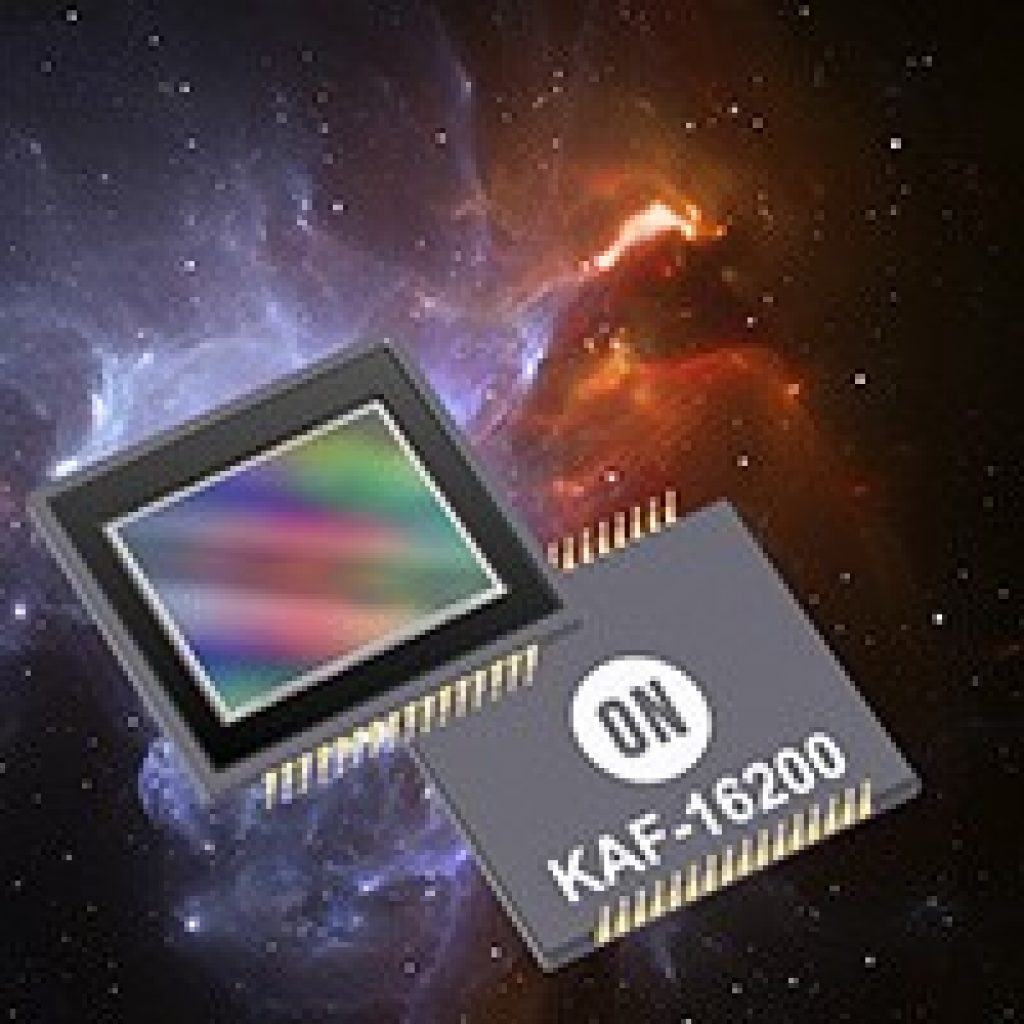
PHOENIX, AZ – Nov. 17, 2015 – ON Semiconductor (Nasdaq: ON), driving energy efficient innovations, is advancing image capture for demanding astrophotography and scientific imaging applications with availability of a new 16.2 megapixel (MP) charge-coupled device (CCD) image sensor.
The new KAF-16200 CCD image sensor leverages the advanced design and manufacturing capabilities of ON Semiconductor to enable image capture of the highest quality. The device’s Full Frame CCD architecture provides best in class image uniformity and dark current, and the use of 6.0 micrometer (µm) pixels with a transparent gate electrode provides high sensitivity, high dynamic range, and integrated overexposure protection. Together, these allow the KAF-16200 to provide exceptional imagery and detail in an APS-H (34.6 mm diagonal) optical format.
“This new image sensor targets opportunities directly identified by our camera manufacturing customers,” said Herb Erhardt, Vice President and GM, Industrial and Security Division, Image Sensor Group at ON Semiconductor, “The KAF-16200 provides a 2x increase in resolution compared to our current device addressing this segment, without sacrificing the CCD-level image quality required for these applications. This is another example of ON Semiconductor’s ability to leverage a broad technology base to provide the highest quality image sensor devices regardless of the underlying technology.”
The KAF-16200 is available in a RoHS-compliant CERDIP package, and is available in both monochrome and color configurations.
Follow @onsemi on Twitter: www.twitter.com/onsemi
About ON Semiconductor
ON Semiconductor (Nasdaq: ON) is driving energy efficient innovations, empowering customers to reduce global energy use. The company is a leading supplier of semiconductor-based solutions, offering a comprehensive portfolio of energy efficient power and signal management, logic, standard and custom devices. The company’s products help engineers solve their unique design challenges in automotive, communications, computing, consumer, industrial, medical and military/aerospace applications. ON Semiconductor operates a responsive, reliable, world-class supply chain and quality program, and a network of manufacturing facilities, sales offices and design centers in key markets throughout North America, Europe, and the Asia Pacific regions. For more information, visit http://www.onsemi.com.