This article was originally published as a two-part blog series at Aldec's website. It is reprinted here with the permission of Aldec.
It's pretty hard to overestimate the role of heterogeneous embedded systems based on Xilinx® Zynq®-7000 All-Programmable devices in tasks like computer vision. Many consumer electronics and specialized devices are emerging to facilitate and improve industries such as medical, automotive, security, and IoT. Aldec delivers Zynq-based SoC FPGA embedded hardware platforms with our TySOM™ Embedded Development Kits to solve the complicated problems associated with this emerging market. Check out the official press release if you have missed it.
The combination of high-performance ARM® application processing and Xilinx programmable FPGA fabric turns the whole development process into a series of easy and efficient design steps. Computer vision engineers are able to choose the design flow that suits their needs: pure CPU application using popular computer vision libraries, pure RTL design in FPGA, or a mixed flow using the best from both worlds.
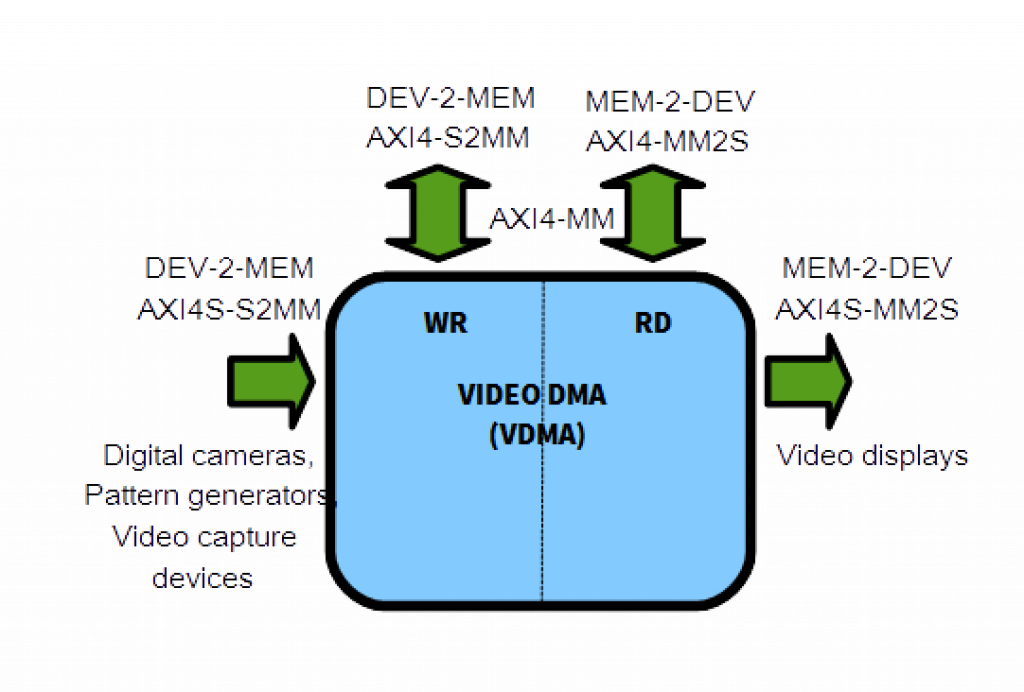
But what is behind the scenes? Designers require an image source (input) as well as an image visualization device (output) to check the results of the image processing algorithm. Typically, these are digital cameras and display panels. In general, an image processing algorithm implies the pixel data is stored into frame buffers allocated in main system DDR memory. But how should that data get to memory? How does the input from a camera ultimately reach the output on a display as a processed image? Introducing the Xilinx VDMA IP core.
VDMA stands for Video Direct Memory Access and is nothing but a modification of a general-use DMA engine for video/imaging applications. VDMA is used to get the pixel data from image source devices to the memory (write channel) or move that data from memory to the image displays (read channel). So let's see how it's actually done.
Video Input Subsystems
A video input subsystem is a set of IP cores used to grab, convert and store the image data into the memory buffers. The write channel of the VDMA engine takes the pixel data represented in AXI4-Stream form and translates it into a series of the incoming burst DDR transfers using AXI4-MM (Memory Mapped) protocol. As it follows from the description above, the initial pixel data must use an AXI4-Stream format which is a non-addressable modification of the standard AXI4 protocol for high-speed data transfers between image source/destination devices and the data processors. The VDMA engine recognizes the AXI4-Stream TUSER signal as SOF (Start Of Frame) as well as the TLAST signal as EOL (End Of Line), both of which are required for frame synchronization purposes. The pixel data comes through TDATA lines strobed by the TKEEP signal. A simple TVALID/TREADY handshake is used to synchronize the slave and master devices similarly to the MM version of AXI4 protocol conventions.
![]()
Video frame transfer over AXI4-Stream protocol (image source: www.xilinx.com)
Sometimes it can be a little bit tricky to convert the input data from camera sensor into the streaming format which is shown in the next 2 cases of frame grabbing used for TySOM reference designs reviewed below.
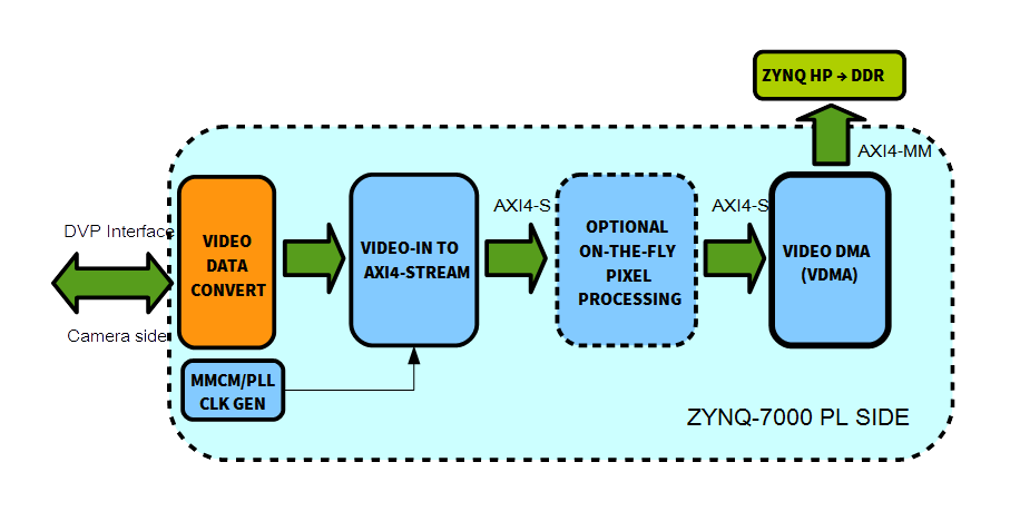
Parallel camera interface: Digital Video Port (DVP)
Target HW platform: TySOM-2-7Z045 & FMC-ADAS + Blue Eagle HDR camera
 Digital CMOS camera with a parallel DVP interface is a well-known image source for an advanced Zynq designer and is well suited for low-resolution solutions (up to 1 Mpx). It's easy to use with Zynq because the raw pixel data is present on the camera interface data lines along with the line (HREF) and frame (VSYNC) synchronization signals. Each portion of pixel data is sampled by the pixel clock (PCLK) present on the interface. Actually that is the main limiting factor: growing image sensor resolution will result in a linearly growing pixel clock frequency making the data on lines unstable and hard to use. Zynq designer may meet a need to convert HREF signal into HSYNC form as well as a need for an additional clocking scheme. Such a subsystem is widely used for Aldec's Automotive Solutions reference designs and the VDMA engine as the heart of the video input subsystem makes it possible.
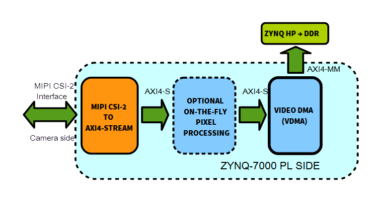
Serial camera interface: MIPI CSI-2
Target HW platform: TySOM-1-7Z030 + RaspberryPi camera v1.3
 When image sensor performance is increasing into the values above 1-2 megapixels, MIPI CSI-2 serial camera interface is there to help. In this case, pixel data and clock are distributed via differential lanes in a serial manner. The CSI-2 protocol can work in 2 modes: High Speed (HS) for an image payload transmission and Low Power (LP) for a backside data payload transmission through the same data lines. Yes, this makes the receiver device logic more complicated. But, on the bright side, there is no strict limitation for camera sensor performance allowing expansion of an image size up to 10-16 megapixels and more. Although the Zynq-7000 devices are not fully electrically compatible with the MIPI D-PHY physical protocol used for CSI-2, those data lines can be accessed by Zynq using the LVDS I/O standard running in HS mode. The RaspberryPi camera is a typical device which utilizes CSI-2 equipped image sensors and is used for IoT and embedded vision reference designs available for Aldec’s TySOM EDK. VDMA helps to bring the data received and converted into the DDR allocated frame buffers.
Video Output Subsystems
A video output subsystem, similar to the previously described video input subsystem, is a set of IP cores used to move pixel data from the memory allocated buffers to the video display device interface including colorspace and pixel format conversions if needed. The read channel of a VDMA engine takes the pixel data represented in AXI4-MM format and translates it into a series of outcoming burst DDR transfers to the AXI4-Stream data sink. The main distinction here is a need for pixel clock and video timing generation on the FPGA. Considering the possible support for multiple video screen resolutions, the pixel clock/video sync generation logic should contain an option for realtime reconfiguration for changing resolutions. Additionally, multiple output video streams may be layered together using an appropriate IP core to produce multi-layered video.
High resolution (high speed) video panel: HDMI display
Target HW platform: TySOM-1-7Z030 and TySOM-2-7Z045
_video_panel2.png) The most frequently referenced and de-facto standard piece of hardware for HDMI screen interfacing projects is the AD7511 transmitter module manufactured by Analog Devices (AD). It's used to convert parallel video data into the serial TMDS standard implemented by the HDMI data transmission protocol. Although AD is sharing their own reference design for AD7511 interfacing, the same job can be done using standard Xilinx IP cores from the Vivado IP Catalog. Aldec provides TySOM Ubuntu Embedded Host reference designs based on an AD framework, as well as reference designs equipped with the HDMI video output subsystems based on Xilinx IP cores only. Both approaches benefit from a VDMA read channel implementation.
The most frequently referenced and de-facto standard piece of hardware for HDMI screen interfacing projects is the AD7511 transmitter module manufactured by Analog Devices (AD). It's used to convert parallel video data into the serial TMDS standard implemented by the HDMI data transmission protocol. Although AD is sharing their own reference design for AD7511 interfacing, the same job can be done using standard Xilinx IP cores from the Vivado IP Catalog. Aldec provides TySOM Ubuntu Embedded Host reference designs based on an AD framework, as well as reference designs equipped with the HDMI video output subsystems based on Xilinx IP cores only. Both approaches benefit from a VDMA read channel implementation.
Low resolution (low speed) video panel: parallel data LCD screen
Target HW platform: TySOM-1-7Z030
_video_panel.png) LCD touch panels are widely used for smartphone industry touch screen based user environments like Android OS or touch screen driven versions of Linux OS distributions like Ubuntu Phone. The TySOM-1-7Z030 development board is a great hardware platform if you require touchscreen functionality with Zynq. Utilizing touchscreens is easy with the LCD-based Ubuntu Embedded Host TySOM-1-7Z030 reference design. It implements hardware and software support for LCD touchscreens for convenient interfacing with the Zynq processing system.
LCD touch panels are widely used for smartphone industry touch screen based user environments like Android OS or touch screen driven versions of Linux OS distributions like Ubuntu Phone. The TySOM-1-7Z030 development board is a great hardware platform if you require touchscreen functionality with Zynq. Utilizing touchscreens is easy with the LCD-based Ubuntu Embedded Host TySOM-1-7Z030 reference design. It implements hardware and software support for LCD touchscreens for convenient interfacing with the Zynq processing system.
All Together Now (Conclusion)
Both VDMA channels can be used simultaneously by the same VDMA engine which provides incredible efficiency. The main goal of such a configuration is an attempt to reduce the amount of FPGA resources required for video input/output subsystems implementation. Using the single VDMA engine for both input and output shrinks the size of the design and decreases power consumption.
Leveraging the power of the VDMA engine provided by Xilinx’s IP Catalog is a step toward successful and efficient Zynq-7000 based application design. The freedom from worrying about your direct memory access system allows you to stay focused on your computer vision application deployment instead of wasting your time trying to figure out why the data is not passing the way you expect.
Understanding Aldec TySOM EDK VDMA-centric reference designs may save you development time, reduce time-to-market, and generally increase the overall efficiency of your embedded design.
To learn more about TySOM High-Performance Embedded Development, visit www.aldec.com/products/tysom.
Igor Gorokhov
Embedded Systems Engineer, Aldec