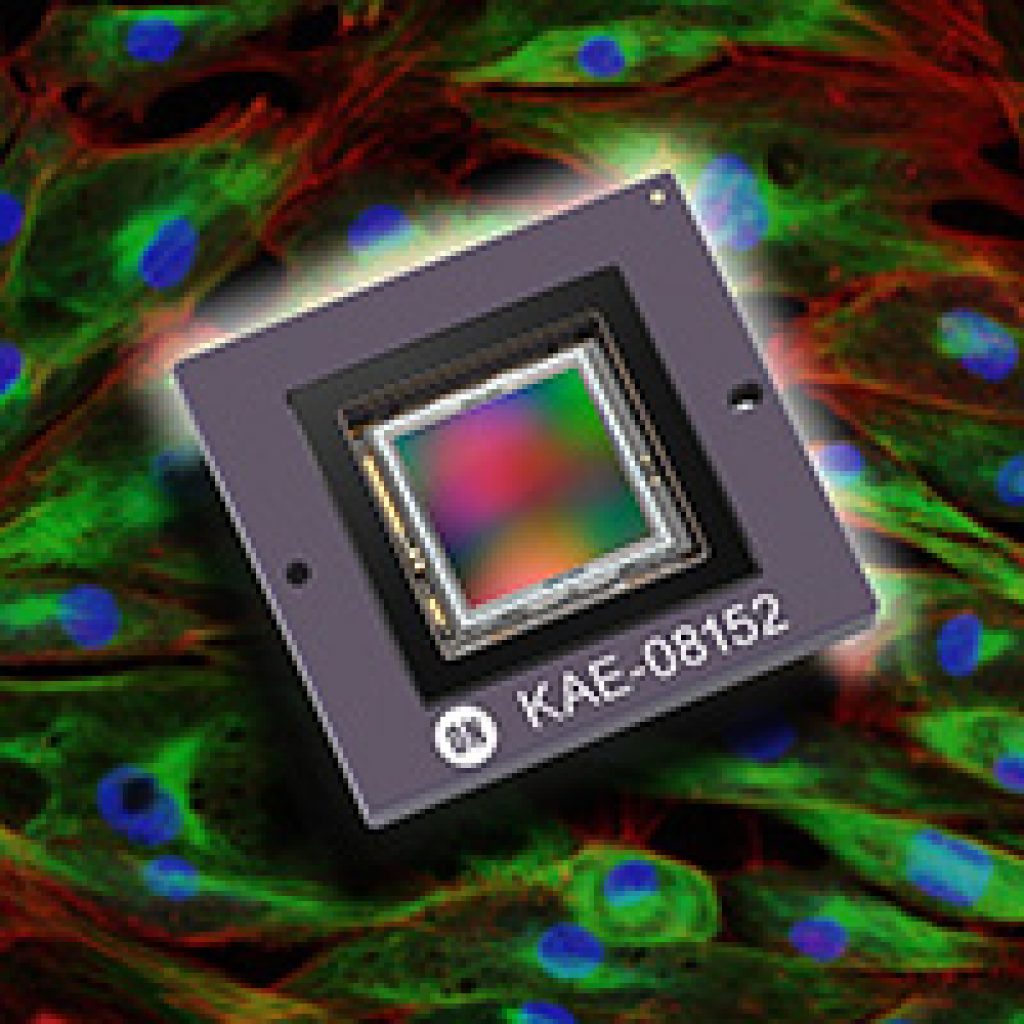
Enhanced NIR sensitivity and integrated cooler improve performance and simplify development for camera manufacturers
PHOENIX, Ariz. – April 3, 2018 – ON Semiconductor (Nasdaq: ON), driving energy efficient innovations, has announced the latest additions to its portfolio of Interline Transfer Electron Multiplying CCD (IT‑EMCCD) image sensors that target extreme low-light applications such as medical and scientific imaging, as well as commercial and military applications for high-end surveillance.
The new KAE-08152 shares the same 8.8 megapixel resolution and 4/3 optical format as the existing KAE-08151, but incorporates an enhanced pixel design that doubles Quantum Efficiency for near-infrared (NIR) wavelengths such as 850 nm – an enhancement which can be critical in applications such as surveillance, microscopy, and ophthalmology. The KAE-08152 is fully drop-in compatible with the existing device, simplifying adoption for camera manufacturers.
In addition, all devices in ON Semiconductor’s IT-EMCCD portfolio are now available with packages that incorporate an integrated thermoelectric cooler. This option addresses the increased effort and potentially higher costs that camera manufacturers can incur when developing a cooled camera design in order to fully maximize the performance of these devices.
“Interline Transfer EMCCD technology enables image capture with video frame rates even under extreme low-light conditions – down to moonless starlight,” said Herb Erhardt, Vice President and General Manager, Industrial Solutions Division, Image Sensor Group at ON Semiconductor. “With new options that provide enhanced NIR sensitivity and integrated cooling, this expanded portfolio allows customers to identify the best low-light imaging solution for their application.”
Interline Transfer EMCCD devices combine two established imaging technologies with a unique output structure to enable a new class of low-noise, high-dynamic range imaging. Interline Transfer CCD provides excellent image quality and uniformity with a highly efficient electronic shutter, while EMCCD excels under low-light conditions. Combining these technologies allows the low-noise architecture of EMCCD to be extended to multi-megapixel resolutions, and an innovative output design allows both standard CCD (normal-gain) and EMCCD (high-gain) outputs to be utilized for a single image capture – extending intrascene dynamic range and scene detection from sunlight to starlight in a single image.
Engineering grade versions of the KAE-08152 are now available, with production planned for 2Q18. KAE‑04471 and KAE-08151 devices with integrated TEC coolers will be in production in 2Q18, while cooled versions of the KAE-02150 and KAE-02152 are available today. All IT‑EMCCD devices ship in ceramic micro-PGA packages, and are available in both Monochrome and Bayer Color configurations. The KAE‑02152 is also available with the Sparse CFA color pattern.
Evaluation kits are available that allow the full performance of this technology to be examined and reviewed under real-world conditions. Customers can purchase an evaluation kit, or enquire about an on-site demonstration of IT-EMCCD devices, by contacting their local ON Semiconductor sales representative.
ON Semiconductor will demonstrate its portfolio of Interline Transfer EMCCD products at both The Vision Show April 10 – 12 in Boston, MA (booth 207) as well as SPIE Defense + Commercial Sensing April 17 – 19 in Orlando, FL (booth 1430).
About ON Semiconductor
ON Semiconductor (Nasdaq: ON) is driving energy efficient innovations, empowering customers to reduce global energy use. The company is a leading supplier of semiconductor-based solutions, offering a comprehensive portfolio of energy efficient, power management, analog, sensors, logic, timing, connectivity, discrete, SoC and custom devices. The company’s products help engineers solve their unique design challenges in automotive, communications, computing, consumer, industrial, medical, aerospace and defense applications. ON Semiconductor operates a responsive, reliable, world-class supply chain and quality program, a robust compliance and ethics program, and a network of manufacturing facilities, sales offices and design centers in key markets throughout North America, Europe and the Asia Pacific regions. For more information, visit http://www.onsemi.com.
- Follow @onsemi on Twitter.


