This market research report was originally published at Yole Développement’s website. It is reprinted here with the permission of Yole Développement.
Four months ago, Yole Développement (Yole) released our Status of CMOS Image Sensor Industry 2020 report, in which we stated that the CIS industry overheated in 2019, reaching a total value of $19.3B. We analyzed the complete ecosystem, wondering if we were heading toward a soft landing in 2020-2021. To know this, it is important to analyze the market, the trends, the industrial landscape, and the technological landscape. The latter is important as there is an explosion in diversity of CIS technology. And we believe new technologies will mean opportunities for new entrants to beat the incumbents, starting a new market cycle.

In that context, we wanted to ask a leading research center in the CIS ecosystem where they were in terms of innovation, targeted applications, roadmaps, and partnerships, to try and get a feel for the potential that is yet to come. Dr. Agnès Arnaud, head of the Optics and Photonics Department at CEA-Leti, kindly accepted to share her views and opinions with Zine Bouhamri, Team Lead Analyst, Imaging and Display within the Photonic & Sensing Division at Yole. Please read their discussion below.
Yole Développement (YD) : Could you introduce the CEA-Leti Optics and Photonics Department that you are leading?
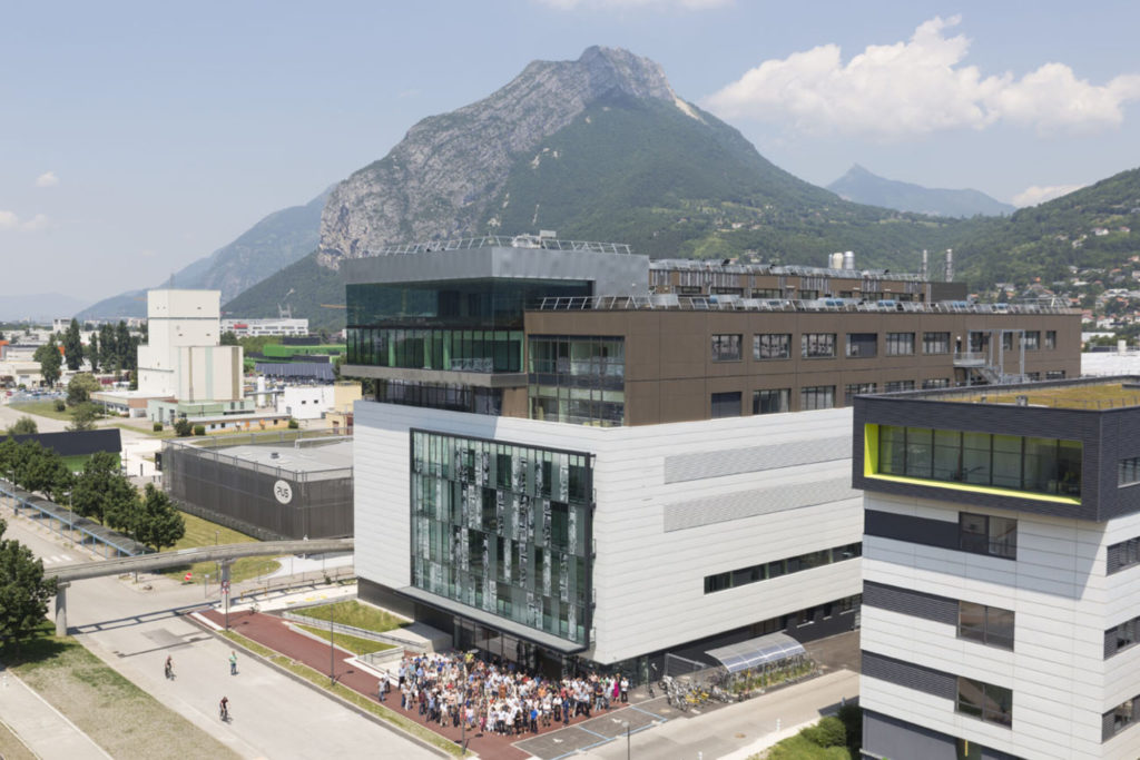
Agnès Arnaud (AA) : The Optics and Photonics Department was created in 1978. It tackles the biggest photonic markets, including imaging from terahertz frequencies to infrared (IR) and visible light, silicon photonics for datacoms and related applications, optical environmental sensors and displays. CEA-Leti’s multidisciplinary know-how ensures innovation in sensors, vision modules and systems to meet challenges raised by every stakeholder from component manufacturer to end user. A laboratory dedicated to visible image sensing was created in 2011. With a portfolio of 700 patents and more than €70 million annual external resources used to maintain world-class infrastructure, the division is committed to ensuring that its teams offer their industrial partners ethical research and excellence. This Optronic Department brings together more than 300 researchers involved in the conception and production of photonic devices and integrated systems in the fields of imagers, displays, communication systems and sensors. It publishes 140 scientific papers per year on optics and photonics.
YD: What is your research and development roadmap in terms of imaging activities?
AA: We increasingly work on high added-value photonic sub-systems that require the coupling between integrated circuit (IC) design and optics and new optic architectures. We work both on the integration of optical functions requiring readout IC (ROIC) design, modeling and simulation, and image processing. Artificial Intelligence (AI) is a strategic program at CEA-Leti. Our design team can ensure every development aspect from the CMOS ROIC close to the pixel signal to advanced embedded software.
Our visible image sensor roadmap is driven by sensitivity increase but we have a roadmap on pixel architecture too. For 2D vision, there is a common trade-off between performance and size, weight, power and cost, or SWAP-C.
We see an extension of our innovations in the fields of photonic applications, such as curved imagers to improve image quality, microLED displays, lidars, integrated depth sensors and lensless microscopic imaging in the mid-infrared. We also explore new pathways such as perovskites for X-ray detection or plenoptic red/green/blue plus depth (RGB+Z) sensing for example.

Grenoble Imaging Valley | CEA-Leti
YD: Could you give us a recap on the partnerships you have established, based on your activities?
AA: CEA-Leti is based in Grenoble in the Imaging Valley. The region of Grenoble has an enviable concentration of diverse R&D labs, dynamic manufacturing companies, higher education institutions, and deep-tech startups. All of them welcome the opportunity to collaborate to create solutions to the technological, scientific, and health-care challenges and opportunities. CEA-Leti’s collaborations include microelectronics labs with STMicroelectronics, Soitec and Applied Materials, work on imagers and infrared with Lynred, Thales and Trixell, and a strong focus on microLEDs and displays with Aledia.
STMicroelectronics is one of the top five companies in the world in CIS. Our partnership requires dedicated efforts and strong involvement from our teams. This is an example of how CEA-Leti builds long-term relationships. Overall, CEA-Leti deals with 250 industrial partners in active bilateral mode. Some names cannot be disclosed but we partner with world leaders in their domains. Our industrial partners can be global companies like STMicroelectronics, Small or Medium sized Enterprises (SMEs), or startups. We strongly support our spinoffs while they grow. Lynred, a global leader in IR imaging technologies, is one of them.
On top of these bilateral relationships, CEA-Leti develops collaborative business models.
CEA-Leti is also part of the IRTNano consortium. The 3D integration program of the IRTNano started in 2012 with three partners including STMicroelectronics. The 3D program grew to six partners at the end of 2019 with the arrival of Prophesee, a French start-up specializing in event-based image sensors, and Aledia, a CEA-Leti spinoff specializing in displays. In 2020, Lynred also joined the consortium.
YD: In all the innovations you are developing, such as organic photodiodes or red/green/blue/infrared filters, are some of them already available on the market? What kinds of markets are they targeting?
AA: CEA-Leti has been involved in CIS development since the mid-1990s. In the early 2000s, CEA-Leti had patents on CIS, including Analog-to-Digital Converters (ADCs), demoisaicing architectures and compression schemes. Some of these technologies have been transferred to the imaging division of STMicroelectronics. STMicroelectronics and CEA-Leti have cooperated for several years on technologies, leading to a boom in imaging applications for mobile telephones. CEA-Leti provided STMicroelectronics with a Through-Silicon-Via (TSV) technology block and processes to make thinner imagers, boost photon collection efficiency and develop innovative architectures. In 2012, a first scientific publication on a Global Shutter Pixel triggered a long-term collaboration on pixel technologies with the imaging division of STMicroelectronics. The cooperation is still on going on advanced concepts, from technologies like dense 3D interconnect announced at IEDM in 2019 to architectures like autonomous imagers announced at VLSI 2020.

“A 3.0µW@5fps QQVGA self-controlled wake-up imager with on-chip motion detection, auto-exposure and object recognition” CEA-LETI – STMicroelectronics joint publication at VLSI 2020
Apart from STMicroelectronics, CEA-Leti has transferred many key technology innovations to world image sensor industrial leaders, addressing market segments like the Internet of Things (IoT), smart home, transportation, medical devices, security, industrial control or space.
We are actively transferring technologies in the infrared domain too.
Leti has been developing bolometric imagers since 1992 and transferred the technology to start-up Ulis in 2002. Ulis, now Lynred, is a world leading bolometer manufacturer. Infrared cameras, whether they are used to keep an eye on city streets or factories, help drivers see better at night, or check a building’s insulation for heat loss, use bolometric imagers.
You must keep in mind that many innovations require 15 to 20 years before one can find them in a commercial product. Our PhD students are currently working on innovations which may show up in a product in 2040.
YD: A few years ago you developed a 3-Tap architecture for 3D sensing. What are the advantages in terms of performance, cost and integration, compared to the other time of flight (ToF) technologies on the market?
AA: You refer to a key scientific paper on transfer gates (TGs), which was published back in 2017. Together with Institut des Nanotechnologies de Lyon, we developed a novel pixel structure for depth map acquisition using a pinned photodiode, fully depleted memories and operating with a four transistor (4T) reading architecture. Time-of-flight can be based on a continuous wave modulation with implementation of a multi-tap approach. CEA-Leti has developed a time-of-flight pixel with implementation of 3-tap phase-shifting technique.
The advantage of this architecture was the integration of depth and color pixel in the same die to achieve a standalone RGB+Z camera. Integration of buried-channel TGs built on a doping-profile-controlled epitaxial layer improves charge-transfer efficiency and speed, which leads to high demodulation contrast.
Simple in its principles, 3D detection is a complex task since the different detection techniques have cons and pros when a practical implementation is considered. There is not one single technology that can handle all applications, ranges, and resolutions.
Particularly through its ongoing collaborations, CEA-Leti provides technological blocks in each of the main principles of 3D detection, direct ToF, indirect ToF and structured light.
CEA-Leti occupies a central role in the Vizta project coordinated by STMicroelectronics. This Electronic Components and Systems for European Leadership (ECSEL) project runs until October 2023. The objective is to develop innovative technologies in the field of optical sensors for short- to long-range 3D-imaging and to demonstrate their value in several key applications in the automotive, security, smart building, mobile robotics for smart cities and Industry 4.0 sectors. The key differentiating silicon sensing technologies developed in Vizta are innovative sensors for Single Photon Avalanche Diode (SPAD) and lock-in pixels for ToF architectures, on-chip solutions with cost-effective near-IR (NIR) and RGB-Z filters, complex RGB+Z pixel architectures for multimodal 2D/3D imaging and many other innovations.

Diffractive Lenses for SPAD – (photo – crédits CEA)
YD: Still referring to your 3D sensing efforts, you mention the potential benefits of germanium-based solutions. Do they improve performance and cost, and can we imagine seeing this in consumer products? Or will it remain a solution for specific applications, such as machine vision or security?
AA: Detection in the short wave IR (SWIR) band is very attractive for various applications, such as military, security, telecommunications and medical diagnostics. The SWIR light presents many advantages compared to visible light. It is invisible to the human eye and is less sensitive to extreme weather conditions such as fog and dust. The use of germanium (Ge) as an active layer in the PiN photodiodes presents many advantages such as its good absorption and its compatibility with the mass-production processes used in the silicon (Si) microelectronics industry. At CEA-Leti, Ge/Si vertical PiN devices have been developed, fabricated, and characterized at room temperature with promising performances such as a low dark current density and good external responsivities. The segmentation of the NIR/SWIR market will ultimately depend on the evolution of InGaAs costs and the improvement of Ge or organic performance. Ge and organic photodiodes are compatible with 300mm diameter silicon wafer production lines. Ge and organic photodiodes are low-cost solutions. Compliance with IC manufacturing make them attractive candidates for consumer products. Yet their intrinsic performance, especially in terms of dark current, is still below InGaAs detectors. And as you know, CEA-Leti is also involved in InGaAs developments. It is CEA-Leti’s mission to investigate the ultimate potential of Ge or organic detectors to offer a reasoned set of technologies.
YD: In the latest Apple product, we have seen image sensors showcasing a technological milestone with in-pixel hybrid stacks. It follows the ever-evolving wafer stacking improvements after Front Side Illumination (FSI), Back Side Illumination (BSI), TSV and hybrid stacking. What do you think about this milestone and what are you looking at for the next step in 3D integration?
AA: Image sensors with 3D stacks are a reality today and Apple products are a good example. 3-layer stacking has been demonstrated by Samsung and Sony, each having their own technological approach, with the integration of a memory layer.
CEA-Leti has been a pioneer in 3D integration for image sensors. CEA-Leti masters technological blocks and investigates the opportunity to embed new functionalities near to the sensor. In coming years, we will see the emergence of vision chips that will no longer manage images but will manage data. Either thanks to fine pitch hybrid bonding or thanks to 3D sequential stacking, dense 3D technologies for pixel architecture will offer unprecedented flexibility to enable higher pixel performance via novel architectures.
Within the IRTNano 3D consortium, CEA-Leti demonstrated a world-class proof of concept, a 3D-integrated image sensor with a connection pitch of 1.4 μm. The publication has received high-profile scientific recognition at the IEEE IEDM and ISSCC meetings.

CEA-Leti Pixcurve technology
YD: Could you please say a word about Pixcurve, your curved image sensor technology?
AA: At CES 2019, CEA-Leti demonstrated a new bioinspired technology for visible image sensors, IR sensors and microdisplays that replicates the curve of the human retina.
This curved image sensor technology breakthrough, called Pixcurve, has several advantages compared to traditional flat image sensors. The form factor of a digital camera module can be reduced by 60% thanks to the reduction of the number of lens elements. The overall length of the optical system is also shorter. Curved image sensors reduce the cost of the camera module. Reducing the number of lens elements and eliminating aspheric lens elements, lowers the cost of systems integrating Pixcurve technology.
On top of this, the quality of the image is improved. Curved image sensors reduce—and in some cases completely eliminate—optical aberrations like curvature of field and the vignetting effect. They also deliver increased brightness and a wider field of view.
A lot of markets could be targeted by Pixcurve approach, such as high-end photography, automotive, consumers application or medical.
Interviewee:
Agnès ARNAUD
Head of the Optics and Photonics Department, CEA-Leti
Interviewer:
Zine Bouhamri, PhD.
Team Lead Analyst, Imaging & Display, Photonic & Sensing Division, Yole Développement (Yole)