This blog post was originally published at Synopsys’ website. It is reprinted here with the permission of Synopsys.
Artificial intelligence (AI) algorithms thirsting for higher performance per watt have driven the development of specific hardware design techniques, including in-memory computing, for system-on-chip (SoC) designs. In-memory computing has predominantly been publicly seen in semiconductor startups looking to disrupt the industry, but many industry leaders are also applying in-memory computing techniques under the hood.
Innovative designs using in-memory computing are intending to disrupt the landscape of AI SoCs. First let’s take a look at the status-quo that startups using in-memory computing intend to disrupt. AI hardware has taken a huge leap forward since 2015 when companies and VCs started investing heavily into new SoCs specifically for AI. Investment has only accelerated over the past 5 years, leading to many improvements in AI hardware design for industry leaders. Intel’s x86 processors have added new instructions and even a separate NPU engine. Nvidia has added specific Tensor Cores and forsaken GDDR to implement HBM technologies to increase memory bandwidth. Google has developed specific ASIC TPUs, or Tensor Processing Units, dedicated to AI algorithms (Figure 1). But even though these architectures continue to improve, investors are looking to startups to develop the next disruption in AI technology.
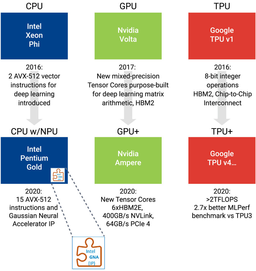
Figure 1: Intel, Nvidia and Google are introducing new hardware architectures to improve performance per watt for AI applications
Why are Disruptions for AI Compute so Interesting?
The three key reasons for heavy investment into AI hardware are: 1) the amount of data generated is growing exponentially and AI is the critical technology to address the complexity; 2) the costs of running AI algorithms in power and time are still too high with existing architectures, specifically at the edge; 3) the parallelization of AI compute engines is reaching die size limits, driving these systems to scale to multiple chips which is only practical in cloud or edge-cloud data centers. Together, these new challenges are driving designers to explore new, innovative hardware architectures. In-memory compute is looked upon as one of the most promising hardware innovations because it may provide multiple orders of magnitude in improvements.
Paths for AI Compute Disruption
Startups and leading semiconductor providers are looking at potential paths for AI compute acceleration.
- New types of AI models: New neural networks are being introduced quite often. For example, Google’s huge research team dedicated to releasing models has produced EfficientNet. Advanced Brain Research has released the LMU, and Lightelligence has partnered with MIT to run Efficient Unitary Neural Network (EUNNs).
- Integrated photonics is being explored by several startups as another method for disruption.
- Compression, pruning and other techniques are being developed to enable specific AI functions to operate on small, efficient processors such as a DesignWare® ARC® EM Processor IP running under 100MHz.
- Scaling compute systems by packaging multiple die, multiple boards, or multiple systems is already in full production from the industry leaders. This solution is used to solve the most complex, costly challenges with AI.
These methods to increase performance are all being pursued or already realized. In-memory computing designs can build on these methods to drive efficiencies with multiple times improvements in addition to the other developing technologies.
What is In-Memory Computing?
In-memory computing is the design of memories next to or within the processing elements of hardware. In-memory computing leverages register files, memories within processors, or turns arrays of SRAMs or new memory technologies into register files or compute engines themselves. For semiconductors, the essence of in-memory computing will likely drive significant improvements to AI costs, reducing compute time and power usage.
Software and Hardware for In-Memory Compute
In-memory computing includes both hardware and software elements, which can cause some confusion. From a software perspective, in-memory computing refers to processing analytics in local storage. Basically, the software takes full advantage of the memories closer to the compute. “Memories” is a bit vague from a hardware perspective and can refer to DRAMs, SRAMs, NAND Flash and other types of memories within the local system rather than sourcing data over a networked software infrastructure. Optimizing software to take advantage of more localized memories has vast opportunity for industry improvement and teams of engineers will need to continue focus on these innovations at a system level. However, for hardware optimizations, in-memory compute offers bit level innovations that more closely mimic the human brain which is 1000s of times more efficient than today’s compute.
In-Memory Compute, Near-Memory Compute, and Analog Compute
In-memory computing hasn’t just arrived as a magic solution to AI algorithms—it has differing implementations and is evolving from a progression of innovations. The implementation of register files and caches has been around for decades and near-memory computing has been the natural progression of improvement and has seen implementations in new SoCs over the past several years. AI algorithms require millions, if not billions, of coefficients and multiply-accumulates (MACs). To efficiently perform all these MACs, customized local SRAMs for an array of MACs are now designed into SoCs for the sole purpose of performing AI model math, i.e., matrix/tensor math. Integrating dedicated specialized local SRAMs for an array of MACs to perform AI model math is the concept of near-memory compute. In near-memory compute, local SRAMs are optimized for the purpose of storing weights and activations needed for their designated MAC units.
The next natural progression to develop in-memory compute is analog computing. Analog computing enables additional parallelism and more closely mimics the efficiencies of a human brain. For analog systems, MACs and memories are parallelized, improving the system efficiency even further than near-memory compute alone. Traditional SRAMs can be the basis for in-memory analog computing implementations and Synopsys has delivered customizations for this very purpose.
Memory Technologies Address In-Memory Compute Challenges
New memory technologies are such as MRAM, ReRAM and others are promising as they provide higher density and non-volatility when compared to traditional SRAMs. Improvements over SRAMs can increase the utilization of the compute and memory on-chip. Utilization is one of the most critical design challenges for AI SoC designers (Figure 2). SoC designers need memory subsystems designed specifically for AI data movement and compute regardless of the technology used.
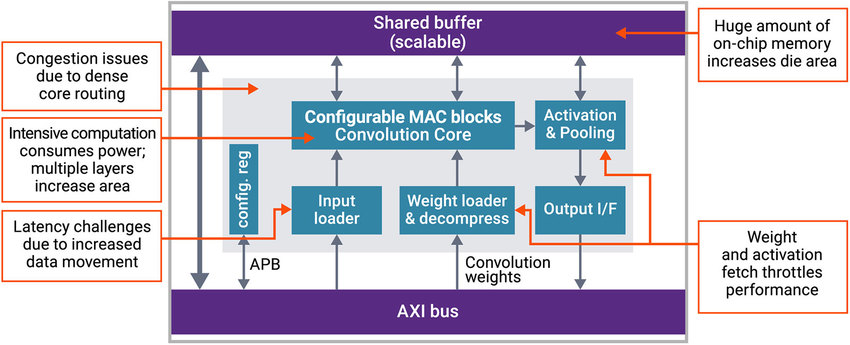
Figure 2: AI SoCs have extremely intensive computation and data movement, which can impact latency, area, and performance
The key challenges for AI SoC design with memory systems relate back to the number of MACs and coefficients that need to be stored. For ResNet-50, over 23M weights are needed and that computes into 3.5 billion MACs and 105B memory accesses. Not all are running at the same time, so the size of the largest activation can be the critical bottleneck to the memory subsystems. Control engineers know that efficiencies are made by designing bottlenecks to be at the most expensive functions of execution. Thus, designs need to ensure that their in-memory compute architectures can handle the largest layer of activation coefficients effectively.
Meeting these requirements demands huge amounts of on-chip memory and intensive computation of the multiple layers. Unique techniques in memory design are being developed to remove latencies, remove the size of coefficients and remove the amount of data that must be moved around the SoC.
DesignWare IP Solutions for In-Memory Compute
Synopsys provides a wide array of IP options for customers to implement in-memory computing. Optimized memory compilers specific for density or leakage are used to develop the local SRAMs for near-memory implementations where sometimes 1000s of MACs are instantiated. MACs can leverage a portfolio of Synopsys Foundation Core primitive math functions that includes flexible functions such as Dot Product, a common AI function.
In addition, Synopsys DesignWare Multi-Port Memory IP enabling up to 8 inputs or 8 outputs improves parallelism within the compute architectures. Multi-port memories are much more common within designs since AI has become so prevalent.
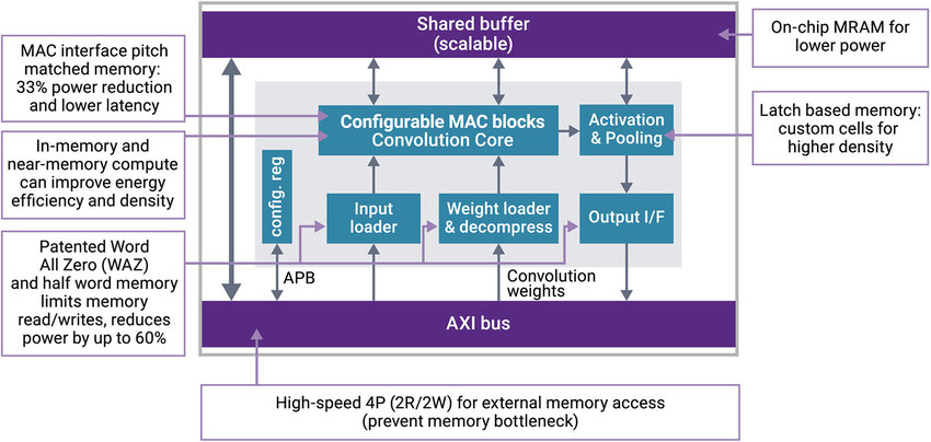
Synopsys developed a patented circuit that demonstrates innovations supportive of in-memory compute. A Word All Zero function, shown in Figure 3, essentially eliminates zeros from being processed. Why move zeros to multiply? The Word All Zero function significantly reduces the compute required and can reduce power by up to 60% for data movement within the chip.

Figure 3: In addition to the Word All Zero function, Synopsys DesignWare Embedded Memory IP offers multiple features to address power, area, and latency challenges
Conclusion
How fast in-memory compute is adopted in the industry remains to be seen; however, the promise of the technology and conceptual implementation with new memories, innovative circuits and creative designers will surely be an exciting engineering accomplishment. The journey to the solution is sometimes as interesting as the final result.
For more information:
- DesignWare IP for AI SoCs
- Video: AI SoC Chats: IP for In-Memory/Near-Memory Compute
- White paper: Neuromorphic Computing Drives the Landscape of Emerging Memories for Artificial Intelligence SoCs
Ron Lowman
Product Marketing Manager, Synopsys