-
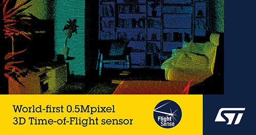
Groundbreaking FlightSense™ 3D sensor augments the imaging capabilities of smartphones, AR/VR equipment, and consumer robots
-
Proprietary indirect Time-of-Flight (iToF) BSI technology on 40nm stacked-wafer delivers high performance with low power and small sensor size
22 Feb 2022 | Geneva, Switzerland | STMicroelectronics (NYSE: STM), a global semiconductor leader serving customers across the spectrum of electronics applications, has announced a new family of high-resolution Time-of-Flight sensors that bring advanced 3D depth imaging to smartphones and other devices.
The 3D family debuts with the VD55H1. This sensor maps three-dimensional surfaces by measuring the distance to over half a million points. Objects can be detected up to five meters from the sensor, and even further with patterned illumination. VD55H1 addresses emerging AR/VR market use cases including room mapping, gaming, and 3D avatars. In smartphones, the sensor enhances the performance of camera-system features including bokeh effect, multi-camera selection, and video segmentation. Face-authentication security is also improved with higher resolution and more accurate 3D images to protect phone unlocking, mobile payment, and any smart system involving secure transactions and access control. In robotics, the VD55H1 provides high-fidelity 3D scene mapping for all target distances to enable new and more powerful capabilities.
“The innovative VD55H1 3D depth sensor reinforces ST’s leadership in Time-of-Flight, and complements our full range of depth sensing technologies,” said Eric Aussedat, ST’s Executive VP, Imaging Sub-Group General Manager. “The FlightSense™ portfolio now comprises direct and indirect ToF products from single-point ranging all-in-one sensors to sophisticated high-resolution 3D imagers enabling future generations of intuitive, smart, and autonomous devices.”
Indirect time-of-flight (iToF) sensors, such as VD55H1, calculate the distance to objects by measuring the phase shift between the reflected signal and the emitted signal. This is a complementary technique to direct time of flight (dToF) sensors, which measure the time for transmitted signals to be reflected back to the sensor. ST’s broad portfolio of advanced technologies enables the Company to design both direct and indirect high-resolution ToF sensors, and offer optimized solutions tailored to application requirements.
VD55H1’s unique pixel architecture and fabrication process, leveraging in-house 40nm stacked wafer technology, ensures low power consumption, low noise, and optimized die area. The die contains 75% more pixels than existing VGA sensors, within a smaller die size.
The VD55H1 sensor is now available for lead customers to sample. Volume production maturity is scheduled for the second half of 2022. A reference design and complete software package are available to help accelerate sensor evaluation and project development.
Further technical information
Featuring a 672 x 804 back-side illuminated (BSI) pixel array for iToF depth sensing, the VD55H1 is the first sensor of its type in the industry.
It has the unique ability to operate with a modulation frequency of 200MHz with more than 85% demodulation contrast at 940nm. This reduces the depth noise by a factor of two over incumbent sensors that typically operate around 100MHz. In addition, multi-frequency operation, an advanced depth-unwrapping algorithm, low pixel noise floor, and high pixel dynamic range ensure superior measurement accuracy over long ranging distance. Depth accuracy is better than 1% and typical precision is 0.1% of distance.
Other features include a short capture sequence that supports a frame rate up to 120 fps and improves motion-blur robustness. In addition, advanced clock and phase management including spread spectrum clock generator (SSCG) provides multi-device interference mitigation and optimized electromagnetic compatibility.
The power consumption can be reduced to less than 100mW in some streaming modes, to help prolong the runtime of battery-operated devices.
A consumer device form factor reference design for the VD55H1 has been created that includes the illumination system. A supporting fully featured software driver and a library containing an advanced depth-reconstruction image-signal-processing pipeline compatible with Android embedded platforms is also provided.
About STMicroelectronics
At ST, we are 48,000 creators and makers of semiconductor technologies mastering the semiconductor supply chain with state-of-the-art manufacturing facilities. An independent device manufacturer, we work with more than 200,000 customers and thousands of partners to design and build products, solutions, and ecosystems that address their challenges and opportunities, and the need to support a more sustainable world. Our technologies enable smarter mobility, more efficient power and energy management, and the wide-scale deployment of the Internet of Things and 5G technology. ST is committed to becoming carbon neutral by 2027. Further information can be found at www.st.com.