This blog post was originally published at Digica’s website. It is reprinted here with the permission of Digica.
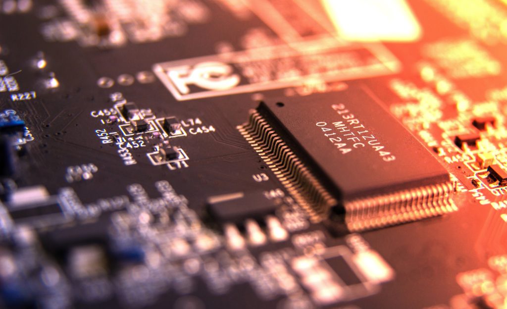
The semiconductor industry stands as a driving force behind technological advancements, powering the devices that have become integral to modern life. As the demand for faster, smaller and more energy-efficient chips continues to grow, the industry faces new challenges in scaling down traditional manufacturing processes.
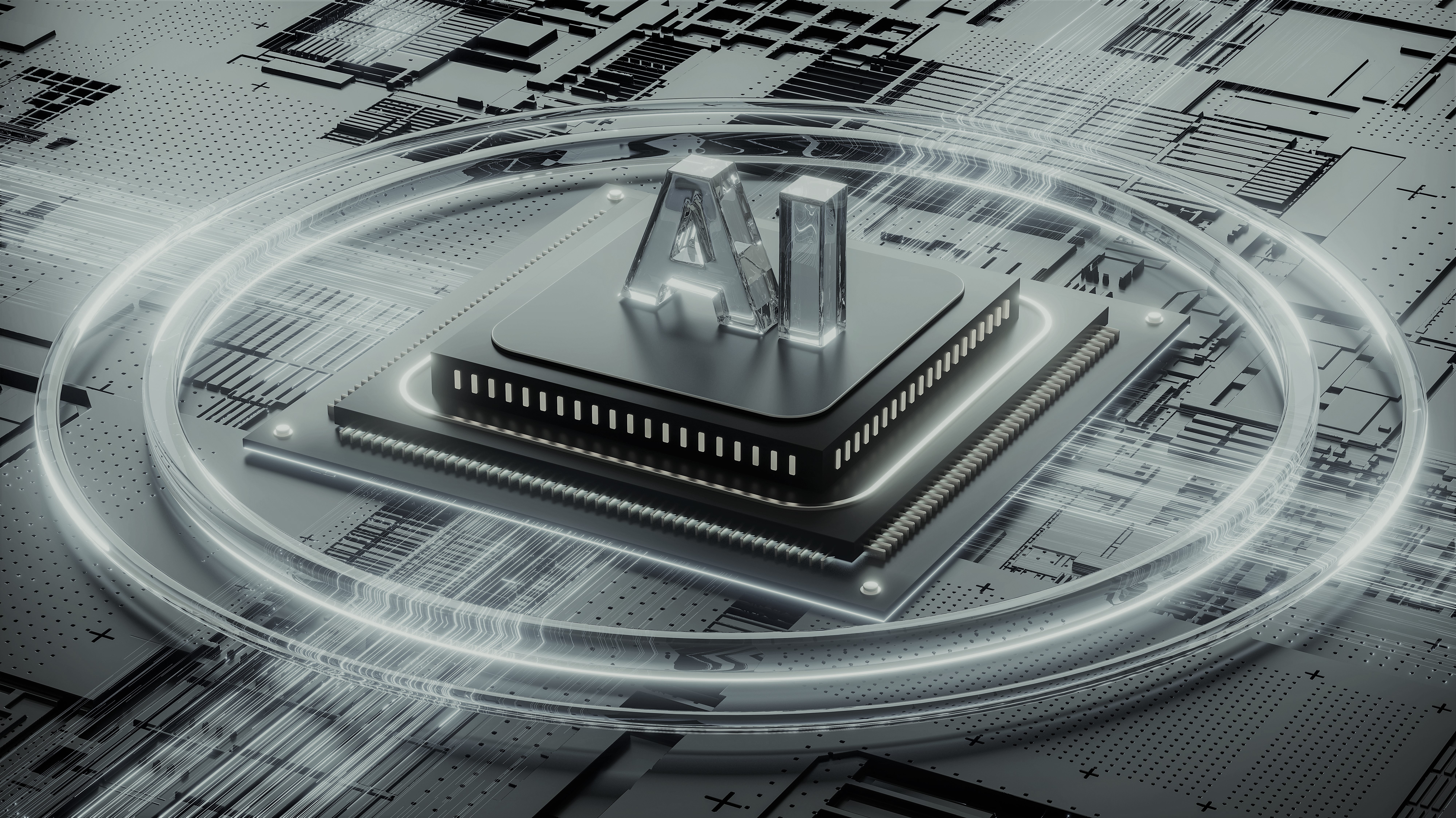
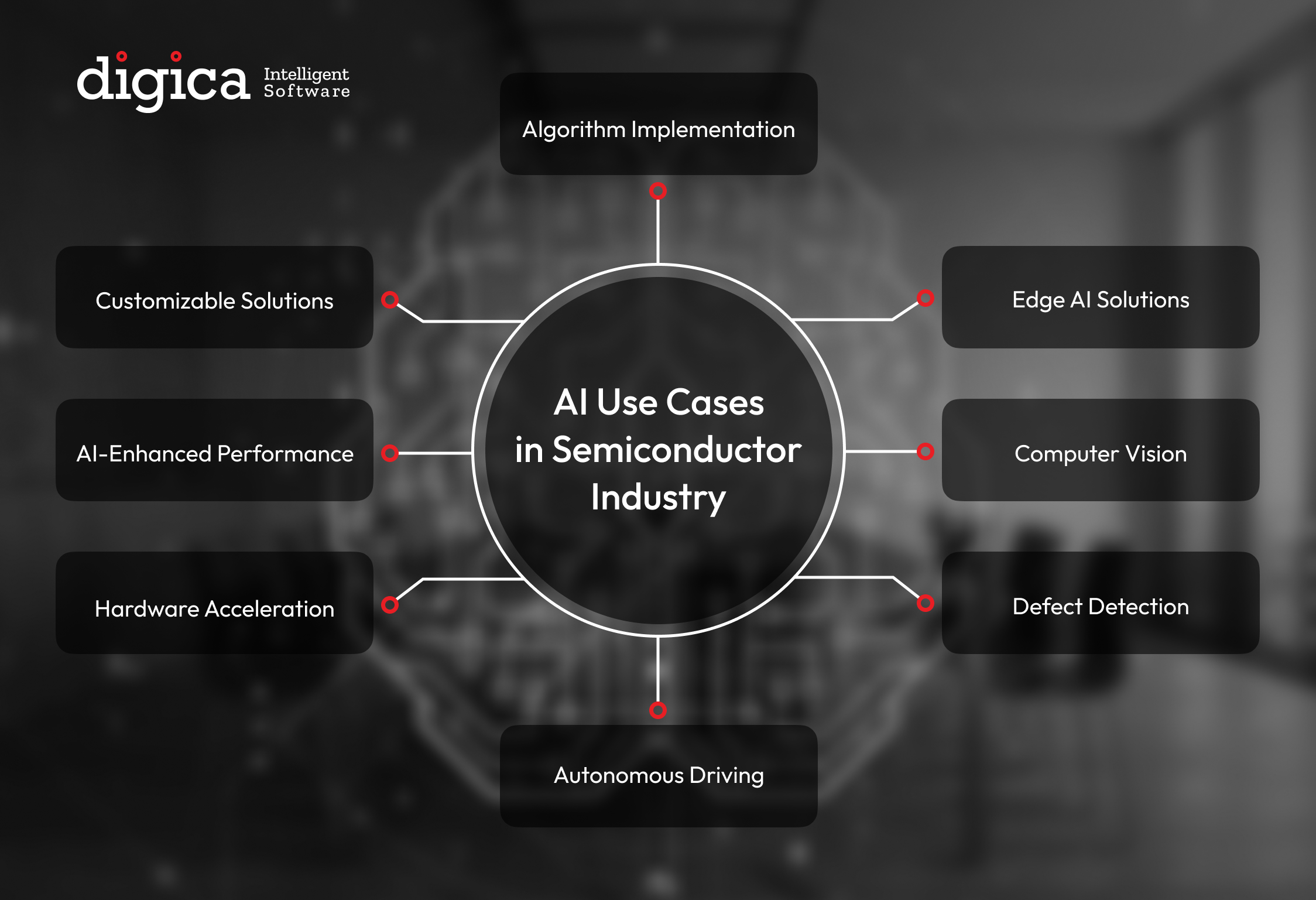
Fortunately, artificial intelligence has emerged as a potent catalyst for transforming the semiconductor landscape. In this article, we will explore how AI is revolutionising the industry, with a focus on hardware acceleration and algorithm implementation to boost AI performance.
Light Detection and Ranging (LiDAR) Point Cloud-processing Algorithms
Algorithms that operate on LiDAR point clouds are a crucial part of the processing performed by a vehicle’s on-board computer. The parallelization and optimization of these algorithms in order to meet latency requirements are of prime importance for real-time systems.
For one of our customers, a leader in semiconductor IP solutions, Digica developed LiDAR point cloud-processing algorithms that were optimised for their GPU. Our objectives in this project were the implementation of point cloud pre-processing “kernels” running on Imagination’s GPU platform using OpenCL, comparison against a reference CUDA implementation, visualisation of the processed point cloud, as well as optimisation and testing on the target hardware platform.
Enhancing Manufacturing and Quality Control
In semiconductor manufacturing, precision is paramount to ensure optimal functionality and reliability. AI-driven systems are transforming manufacturing and quality control by monitoring processes in real-time. Through data analysis and pattern recognition, AI can detect anomalies and predict potential defects, reducing waste and maximising yield.
For example, one of Digica’s customers, a leading producer of medical imaging silicon, wanted to utilise AI to identify structural defects in the silicon production process. Digica helped them by reducing the number of defective wafers that reached the assembly stage, and therefore ensured the production of high-quality medical imaging devices whilst reducing wastage in the process.
Image Reconstruction
Ray tracing is computationally intensive, but AI techniques can be used to improve the performance of ray tracing significantly. Our customer’s initial implementation of a System on a Chip operated on an entire HD image. By dividing the image into tiles, which can be processed in parallel, we improved performance on existing hardware by allowing low quality ray tracing images to be enhanced using neural networks.
Our objectives were to implement a model capable of operating on tiles in parallel and to identify techniques that allow the model to be reduced in size without losing quality compared to the baseline. In order to achieve this, we had to implement baseline knowledge distillation, a trainable filter network and several advanced KD techniques. As a result, we created a tiled model that achieved comparable metrics (LPIPS, SSIM, PSNR) to the reference model.
Optimising Energy Efficiency
Energy efficiency is a critical aspect of modern semiconductor devices, especially in the era of mobile and IoT technologies. AI plays a pivotal role in optimising the energy consumption of chips by analysing power usage patterns and identifying inefficiencies. With this information, AI-driven algorithms can suggest design modifications to minimise power consumption without compromising performance, leading to more sustainable and eco-friendly semiconductor solutions.
Enabling Advanced Chip Architectures
AI is playing a significant role in enabling advanced chip architecture in various ways. For example, machine learning algorithms can analyse and generate designs that meet specific performance, power, and size constraints. AI can explore a wide range of design options and parameters to find optimal solutions that human designers might not be able to discover manually. AI algorithms can also predict the performance of different chip architectures through simulation and modeling. This allows designers to make informed decisions about which architecture to pursue and helps to identify potential bottlenecks or areas for improvement.
Conclusion
The integration of AI into the semiconductor industry is driving a remarkable transformation, redefining the way that chips are designed, manufactured and utilised.
From accelerating chip design and development to optimising energy efficiency and exploring cutting-edge chip architectures, AI’s impact is profound. Moreover, AI’s role in LiDAR point cloud processing, image reconstruction through Knowledge Distillation, identifying structural defects, and implementing image processing algorithms further demonstrates its versatility in addressing diverse challenges across the semiconductor sector. With hardware acceleration through GPUs made by companies such as NVIDIA, Arm, AMD and Imagination Technologies, AI performance is boosted, enabling faster simulations, optimizations, and validation.
As AI continues to evolve and collaborate with specialised hardware, the semiconductor industry is poised to unlock new realms of innovation. Responsible implementation and addressing challenges related to data privacy and security are essential to harnessing the full potential of AI in the semiconductor landscape. Together, AI and the semiconductor industry promise a future where smarter, faster, and more sustainable semiconductor devices become the norm, reshaping technology and driving progress in ways that we could only have imagined until now.
To learn more about our projects, please visit our website dedicated to the semiconductor industry: https://www.digica.com/semiconductor.html
Anna Paluszkiewicz
Marketing Manager, Digica
Anna Paluszkiewicz
Marketing Manager, Digica