The Disaggregation of the Monolith: A New Paradigm Forged by AI’s Demands
The semiconductor industry is navigating its most significant architectural shift in decades, a transition compelled by the relentless demands of Generative AI. The monolithic System-on-Chip (SoC), the reigning paradigm for half a century, is fracturing under the weight of exponentially growing AI models and their insatiable need for memory bandwidth and computational power. This has given rise to a more flexible and economically viable model: the chiplet. While the concept dates to 2014 or before, the need for chiplets has increased dramatically in recent times. While AI processing is a dominant use case, many other applications can benefit once the chiplet ecosystem and costs have improved.
This transition represents a fundamental re-imagining of how complex circuits are designed and manufactured. However, the popular “Lego Block” analogy belies the immense technical and business challenges that underscore the infancy of this new ecosystem. The path to a genuinely open, multi-vendor chiplet marketplace is not a simple assembly job; it is a frontier defined by profound hurdles in reliability, testing, and security that the industry is only now beginning to address.
Still in the First Rodeo
To date, almost all chiplet implementations involve AI accelerators and their interfaces to High Bandwidth Memory, I/O, and optical networking. These are ultra-high value applications where a $50 cost difference does not matter. Even higher-value networking and industrial applications lack this luxury, not to mention automotive or consumer applications. Importantly, no single entity can solve all these problems. It takes an entire ecosystem that cooperates at speed and scale. This level of cooperation does not yet exist in mainstream applications. Later in this article, we describe the differences between AMD’s walled garden, ARM’s open ecosystem, and Nvidia’s managed collaborations.
The GenAI Imperative: Why Monolithic Architectures Are Cracking
At its core, the chiplet concept centers on modularity. Instead of one large, complex chip, engineers can build a system by combining multiple specialized dice in an advanced package. Although this idea has been evolving for years, the rapid growth of Generative AI has transformed it from a strategic option into a necessity. As AI models grow and inference workloads become more demanding – requiring larger context lengths and multimodal capabilities – monolithic designs are hitting fundamental limitations in memory, power, and cost.
The modern AI inference workload is not uniform; it involves a complex interaction between prompt processing (which is compute-intensive) and output generation (which is memory-bandwidth-intensive). No single monolithic architecture can be optimally designed for both tasks. As AI startup d-Matrix emphasizes, a “one-size-fits-all” approach is no longer practical. Chiplets offer a solution by enabling modular architectures where logic, memory, and I/O can be individually optimized and scaled to meet the specific needs of various AI applications, from large frontier models in the cloud to smaller, more efficient reasoning models at the edge. The fundamental challenges of the chiplet era include:
1. The Known Good Die (KGD) and Design-for-Test (DFT) Crisis: The most immediate technical barrier is ensuring each chiplet is free of defects before being sealed in an expensive package. The KGD problem becomes exponentially harder with chiplets. Advanced packaging techniques use interconnect pitches of less than 50 microns, making the physical contacts too fine to be tested with traditional wafer probes. A single faulty, untested chiplet can render a multi-thousand-dollar packaged system useless, creating unacceptable financial risk.
This has ignited a revolution in Design-for-Test (DFT). The industry is reviving and adapting established standards and developing new ones specifically for 3D-ICs, to create standardized digital test access pathways into and through stacked dice. Methodologies like Built-In Self-Test (BIST) for logic and memory are no longer optional but mandatory. EDA giants like Synopsys are providing comprehensive toolchains to manage this complexity, enabling everything from at-speed interconnect testing to in-field monitoring, which is critical for addressing the rising concern of Silent Data Corruption (SDC) in large-scale data centers.
2. Reliability, Availability, and Serviceability (RAS): In a monolithic SoC, RAS is a contained problem. In a multi-chiplet system, especially one with dice from different vendors, it becomes a system-level nightmare. This is particularly acute in the automotive sector, where functional safety (e.g., ASIL-D) is non-negotiable.
New technology to address these issues
As pioneered by Athos Silicon, the multiple-Systems-on-Chip™ (mSoC™) architecture redefines system resilience for safety-critical computing. While most of the industry uses chiplets to boost performance within a conventional PC-like architecture, Athos takes a fundamentally different approach. The mSoC platform distributes execution across multiple redundant chiplets, coordinated by a fault-aware voting mechanism that continuously monitors workload integrity. Unlike monolithic designs, where a single transistor upset can lead to catastrophic system failure, mSoC eliminates single points of failure by isolating faulty chiplets and reassigning their functions in real time. Built to meet ASIL-D and aerospace-grade standards, this architecture enables deterministic and certifiable computing platforms. In fact, the certification of high levels of autonomy in ADAS and robotics may not be feasible without the architectural simplifications and fault containment mechanisms introduced by mSoC. And the certification of high levels of autonomy in ADAS and robotics is likely to require a solution of this sort.
3. Unresolved Business Models and Security: In a multi-vendor system, who is liable if the final part fails? This unresolved business question remains one of the biggest impediments to a truly open ecosystem. Furthermore, security becomes more complex. The system’s Root of Trust (RoT) must be able to extend its authority to third-party chiplets, verifying their identity and integrity through attestation. Establishing common standards for these security and RAS functions is a primary focus of industry bodies and a key area of competition. While its products are not currently in the form of a chiplet, Axiado has made impressive progress in multi-mode security, including Root of Trust.
Interconnects, Packaging, and Testability
The chiplet revolution rests on three critical technological pillars: high-speed interconnects, sophisticated advanced packaging, and a standardized framework for test and serviceability. The development and control of these enabling technologies have become a central battleground for industry dominance.
The Interconnect Imperative and the Rise of UCIe
The performance of any chiplet-based system is gated by the quality of its die-to-die (D2D) interconnect. The need for an open standard gave rise to the Universal Chiplet Interconnect Express (UCIe). Backed by a broad consortium of semiconductor industry leaders, UCIe is the catalyst intended to unlock a vibrant, multi-vendor marketplace. The standard is rapidly evolving to meet the demands of AI. As an example, the UCIe Consortium recently introduced the 3.0 specification with 64 GT/s performance and enhanced manageability, in addition to releasing the 2.0 specification, which adds support for a standardized system architecture for manageability.
As highlighted by Alphawave Semi, the industry is already moving beyond the initial 16-24 Gbps implementations to UCIe 64G, a third-generation IP capable of delivering over 20 Tbps/mm of bandwidth density. This leap in performance is essential for connecting next-generation compute and memory chiplets. The elephant in the room is power consumption. The incredible benefits of LLMs have driven every supplier to the highest performance levels in AI datacenters – at the expense of power. History says this pendulum will swing back. The cost and availability of power are too large. After the initial exuberance of massive LLM training is over, datacenter operators will resist mightily the purchase of high-power components and systems.
The Memory Bottleneck and the Evolution of HBM
High-Bandwidth Memory (HBM) has become the most critical chiplet in any AI accelerator, and the performance gap between compute power (FLOPS) and memory bandwidth is a primary system bottleneck. The evolution of the HBM standard is a direct response to this challenge. The upcoming HBM4 standard will double the I/O width to 2048 bits and push speeds higher, effectively doubling the bandwidth per stack to over 2 TB/s.
High-Bandwidth Memory (HBM) is central to AI accelerators, but system performance is increasingly limited by memory bandwidth rather than compute power. It takes an advanced chiplet-based approach to stack HBM dice and enable high-bandwidth data transfers. To address this, the upcoming HBM4 standard doubles the I/O width to 2,048 bits and bandwidth per stack to over 2 TB/s. A key new trend with HBM4 is the rise of custom HBM, where companies design specialized logic dice beneath the DRAM stack—moving memory controller or compute functions into the HBM base die. By replacing the standard PHY with a direct chiplet interface like UCIe, this approach yields higher bandwidth, lower latency, and greater efficiency than the traditional JEDEC HBM standard.
High-Bandwidth Memory (HBM) is essential for AI accelerators, with memory bandwidth increasingly limiting system performance. The upcoming HBM4 standard addresses this by doubling the I/O width to 2,048 bits and increasing stack bandwidth to over 2 TB/s. A key trend with HBM4 is the rise of custom HBM, where companies integrate specialized logic dice beneath the DRAM stack, such as moving memory controller or compute functions into the base die. This approach, using direct chiplet interfaces like UCIe instead of the standard PHY, improves bandwidth, reduces latency, and enhances efficiency.
Holy Grail: A Standardized Framework for Test and Serviceability
As highlighted by the KGD crisis, a robust test framework is as crucial as the physical interconnects. The industry is building a multi-layered test architecture founded on decades of experience, now adapted for 3D systems. It starts with the old JTAG standard that provides test access, but requires more advanced standards that work with stacked dice and multiple data pathways. The requirements extend to in-field monitoring, which is new to many system and chip designers.
The Battle for Ecosystem Control
As the foundational technologies mature, a strategic battle is unfolding over the business model that will define the chiplet era. Four competing philosophies have emerged, each championed by major industry players.
The Walled Garden with Open Gates: AMD’s Anchor Ecosystem
AMD is promoting a structured, semi-open model built around a central “Anchor Chiplet.” This AMD-designed anchor orchestrates essential system-level functions like power, security, and RAS. It then defines two models for third-party integration: Third-Party Die (TPD), using standard interfaces like UCIe, and Third-Party Adapted die (TPA), which gives a partner’s chiplet premium access to AMD’s proprietary infrastructure, including its high-speed Infinity Fabric, for maximum performance. This strategy creates a curated ecosystem that keeps AMD at the center, ensuring a consistent level of quality and reliability.
The Standards-Based Approach: Arm’s Chiplet System Architecture (CSA)
Arm is championing a more open, standards-based approach. The Arm Chiplet System Architecture (CSA) is a specification that defines how chiplets handle system-level tasks beyond the physical layer. CSA defines the protocols for I/O coherent memory (using AMBA CHI-C2C over UCIe), system control, security, and boot sequences. By standardizing these higher-level functions, Arm aims to create a truly interoperable marketplace. The “Project Leapfrog” initiative, a collaboration between Arm, Samsung Foundry, ADTechnology, and Rebellions, is a real-world demonstration of this multi-vendor ecosystem in action, aiming to build an open AI training platform.
The Fully Open Vision: Tenstorrent’s OCA
Challengers like Tenstorrent are pushing the open model even further. By acquiring Blue Cheetah, an interconnect IP provider, Tenstorrent is not just securing technology for its products but positioning itself as a hub for its Open Chiplet Architecture (OCA). The strategy is to use its IP to attract partners to a fully open ecosystem built on UCIe and the RISC-V instruction set, creating a direct challenge to the proprietary models of incumbents.
Managed Collaboration: Nvidia’s Approach
Nvidia collaborates with third-party chiplet suppliers through its NVLink Fusion program. This initiative marks a significant strategic shift for the company, opening its tightly controlled ecosystem to allow for the integration of external CPUs and custom AI accelerators with its powerful GPUs.
The NVLink Fusion program, unveiled as a key component of Nvidia’s strategy, is designed to enable the creation of semi-custom AI infrastructure. This allows hyperscalers and other large-scale data center operators to tailor their systems with specialized processors while still leveraging Nvidia’s dominant GPU technology. The program has already been joined by industry leaders such as Fujitsu, Qualcomm, MediaTek, Marvell, Alchip Technologies, Astera Labs, Synopsys, and Cadence.
This strategic opening of its platform allows Nvidia to maintain its central role in the AI hardware landscape while offering the flexibility that large-scale customers are increasingly demanding. By fostering a collaborative ecosystem, Nvidia is positioning itself to be the core of a broader range of customized, high-performance computing solutions.
The Acquisition Spree and The New Value Chain
The technical complexities and strategic importance of chiplets have triggered a land grab for foundational IP and talent. This M&A activity is reshaping the semiconductor value chain, creating new opportunities and elevating the importance of specialized innovators.
Anatomy of a Strategic Acquisition: Tenstorrent and Blue Cheetah
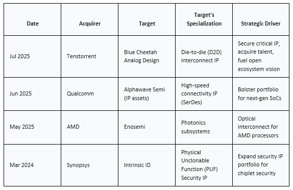
The acquisition of Blue Cheetah by Tenstorrent is a perfect case study. It was a multi-layered move to de-risk its roadmap by internalizing critical D2D interconnect IP, “acqui-hire” a world-class analog design team to fill a key expertise gap, and gain complete control over the technology’s cost and evolution. Most importantly, it was a strategic play to fuel its Open Chiplet Architecture vision by owning the foundational “picks and shovels” needed to build the ecosystem.
The New Chiplet Value Chain and M&A Targets
The chiplet paradigm creates value in new and diverse areas, making companies in these niches essential to consider:
- Interconnect Specialists: Companies like Eliyan and Kandou AI, which provide the critical D2D PHY IP, remain the most sought-after targets.
- Specialized Function Providers (Extreme Heterogeneity): The true power of chiplets is unlocked by integrating diverse technologies.
- Analog/Digital: Companies like Sagence AI are using chiplets to partition their analog in-memory compute engines from their digital control logic.
- Compound Semiconductors: Innovators like PseudolithIC are developing paradigms to integrate compound semiconductor (GaN, InP) chiplets onto standard silicon wafers for high-performance RFICs.
- I/O and Memory Chiplets: Disaggregating I/O into separate chiplets is a significant trend. Companies like Alphawave Semi (acquired by Qualcomm for $2.4B in June 2025) are providing off-the-shelf, multi-protocol I/O chiplets.
- Ecosystem Enablers: A new category of startups is emerging to build the infrastructure for a chiplet marketplace, including companies like Yorchip, Chipletz, and zGlue.
- AMD recently licensed Arteris’ FlexGen network-on-chip (NoC) interconnect IP for its next-gen AI chiplet design, providing high-performance data transport in AMD chiplets to power AI across applications, including data centers, edge, and end devices.
- The acquisition wave has already started, as illustrated by this list of select recent acquisitions:
A New Life for Mature Foundries
Notably, the need for heterogeneous integration creates a significant opportunity for foundries without leading-edge EUV capabilities, such as Tower Semiconductor, SkyWater Technology, and XFab, while considering potential market dynamics. To start, it enables the integration of chiplets from completely different fabrication processes. Importantly, cost factors can be favorable, even with smaller wafer sizes (which are common in older and specialized processes). Why? Die sizes of chiplets are tiny, which increases the number of dice per wafer and improves yields to make them cost-effective in performance-driven applications. This does not solve the issue of testability, but it does make these older processes usable and cost-effective.
For example, SkyWater recently finalized the acquisition of Infineon’s 200 mm facility in Austin, Texas, which it will open to foundry customers. It will increase output for what it calls “foundational” chips on nodes from 130 nm to 65 nm. Customers like Infineon, the Department of Defense (DoD), and even quantum-computing companies like D-Wave are expected to use the fab.
Strategic Implications and the Future Trajectory: The Optical Horizon
The shift towards chiplets and the subsequent consolidation are forging the future of the semiconductor industry. The strategic maneuvers of today are defining the competitive fault lines for the next decade and setting the stage for the next great technological leap in connectivity: the transition from electrical to optical I/O.
The Next Frontier: Scaling with Optical I/O
Even as electrical interconnects like UCIe improve, the rapid growth of large-scale AI systems is pushing them to their physical limits. The power needed to drive high-speed electrical signals across a rack— and the resulting thermal density— is becoming unsustainable. As Ayar Labs points out, the power per rack for GPU systems is expected to skyrocket, creating a “connectivity problem” that electrical I/O cannot solve efficiently.
The solution lies in replacing electrons with photons. Optical I/O, which uses co-packaged optical chiplets to transmit data as light, represents the next frontier. This technology promises a transformative leap in performance, offering:
- Massively Higher Bandwidth Density: Optical waveguides can carry far more data in the same physical space.
- Lower Power Consumption: Transmitting data with light is significantly more energy-efficient, with projections of a 10x improvement at iso-performance.
- Longer Reach: Optical links can efficiently transmit data over hundreds of meters, enabling true resource disaggregation and the creation of vast, coherent compute fabrics that can span multiple racks.
This future is rapidly approaching. Companies like Ayar Labs are already producing reliable, UCIe-compliant optical I/O chiplets and the external laser sources needed to power them. Innovators like Xscape Photonics are developing novel multi-wavelength laser platforms that can further increase bandwidth per fiber by over 10x using Dense Wavelength Division Multiplexing (DWDM). These optical chiplets are the key to breaking the I/O wall and enabling the scalable, flexible, and composable AI infrastructure of the future.
Conclusion and Outlook
The semiconductor industry has embarked on an irreversible journey away from the monolithic chip. Driven by the unyielding demands of AI, the chiplet architecture has moved from a niche concept to the mainstream. This disaggregation has ignited a vibrant ecosystem, but its full potential is constrained by significant challenges in testing (KGD), reliability (RAS), and security.
The acquisition spree is a direct result of these complexities and is set to continue. Well-funded, technologically differentiated startups focused on interconnects, packaging, security, and, increasingly, test and optical I/O solutions, are the most logical targets for the next M&A wave.
Looking ahead, the market will not resolve into a purely “open” or “closed” state. A hybrid model will emerge where large players leverage proprietary solutions for their flagship products while engaging with open standards to tap into a broader ecosystem of innovation. The transition to optical I/O will mark the next great inflection point, promising to shatter current performance barriers. The race to develop and control the key technologies for that optical future has already begun, ensuring that the chiplet consolidation wave is not an endpoint, but merely the beginning of the next chapter in the evolution of silicon.
What will the second and third rodeos look like? We will continue to follow the market and report on the most important developments and trends. Please let us know what’s important to you!
George Jones
Managing Director, Woodside Capital Partners
Alain Bismuth
Managing Director, Woodside Capital Partners
Woodside Capital Partners is one of the leading corporate finance advisory firms for tech companies in M&A and financings in the $30M –$500M segment. The firm has worked with some of the best entrepreneurs and investors since 2001, providing ultra-personalized service to select clients. Our team has global vision and reach, and has completed hundreds of successful engagements. We have deep industry knowledge and extensive domain experience in the following sectors: Autonomous Vehicles and ADAS, Computer Vision, Artificial Intelligence, CloudTech, Enterprise Software, Information Security, Digital Entertainment & Lifestyle, Health Tech, Internet of Things, Networking / Infrastructure, Robotics, Semiconductors, Batteries, Energy Storage, Aerospace and Defense. Woodside Capital Partners is a specialist in cross-border transactions, with extensive relationships among venture capitalists, private equity investors, and corporate executives from global 1000 companies. More about Woodside Capital Partners here.
Questions? Contact George Jones, Managing Director, Woodside Capital Partners at [email protected].