By Paul Zoratti
Driver Assistance Senior System Architect
Automotive Division
Xilinx Corporation
This is a reprint of a Xilinx-published white paper which is also available here (344 KB PDF).
In the last five years, the automotive industry has made remarkable advances in driver assistance (DA) systems that truly enrich the driving experience and provide drivers with invaluable information about the road around them. This white paper looks at how FPGAs can be leveraged to quickly bring new driver assistance innovations to market.
Driver Assistance Introduction
Since the early 1990s, developers of advanced DA systems have striven to provide a safer, more convenient driving experience. Over the past two decades, DA features such as ultrasonic park assist, adaptive cruise control, and lane departure warning systems in high-end vehicles have been deployed. Recently, automotive manufacturers have added rear-view cameras, blind-spot detection, and surround-vision systems as options. Except for ultrasonic park assist, deployment volumes for DA systems have been limited. However, the research firm Strategy Analytics forecasts that DA system deployment will rise dramatically over the next decade.
In addition to government legislation and strong consumer interest in safety features, innovations in remote sensors and associated processing algorithms that extract and interpret critical information are fueling an increase in DA system deployment. Over time, these DA systems will become more sophisticated and move from high-end to mainstream vehicles, with FPGA-based processing playing a major role.
Driver Assistance Sensing Technology Trends
Sensor research-and-development activities have leveraged adjacent markets, such as cell-phone cameras, to produce devices that not only perform in the automotive environment, but also meet strict cost limits. Similarly, developers have refined complex processing algorithms using PC-based tools and are transitioning them to embedded platforms.
While ultrasonic sensing technology has led the market, IMS Research (Figure 1) shows camera sensors dominating in the coming years.
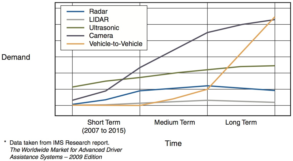
Figure 1. Driver Assistance Sensors Market
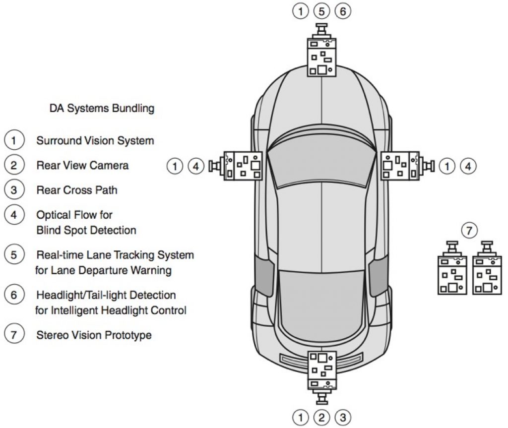
A unique attribute of camera sensors is the value of both the raw and processed outputs. Raw video from a camera can be directly displayed for a driver to identify and assess hazardous conditions, something not possible with other types of remote sensors (for example, radar). Alternatively (or even simultaneously), the video output can be processed using image analytics to extract key information, such as the location and motion of pedestrians. Developers can further expand this "dual-use" concept of camera sensor data by bundling multiple consumer features based on a single set of cameras, as illustrated in Figure 2.
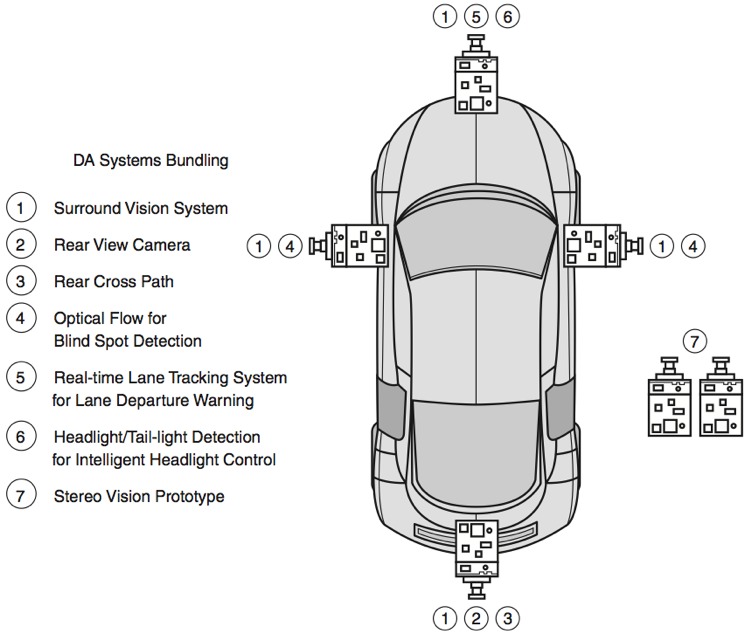
Figure 2. Bundling Multiple Automotive Features
From such applications, it is possible to draw a number of conclusions regarding the requirements of suitable processing platforms for camera-based DA systems:
- They must support both video processing and image processing. In this case, video processing refers to proper handling of raw camera data for display to the driver, and image processing refers to the application of analytics to extract information (for example, motion) from a video stream.
- They must provide parallel datapaths for algorithms associated with features that will run concurrently.
- Given that many new features require megapixel image resolution, connectivity and memory bandwidth are just as critical as raw processing power.
Meeting DA Processing Platform Requirements
FPGAs are well suited to meet DA processing platform requirements. For example, in a wide-field-of-view, single-camera system that incorporates a rear cross-path warning feature, the system's intent is to provide a distortion-corrected image of the area behind the vehicle. In addition, object-detection and motion-estimation algorithms generate an audible warning if an object is entering the projected vehicle path from the side.
Figure 3 illustrates how the camera signal is split between the video- and image- processing functions. The raw processing power needed to perform these functions can quickly exceed what is available in a serial digital signal processor (DSP). Parallel processing along with hardware acceleration is a viable solution.
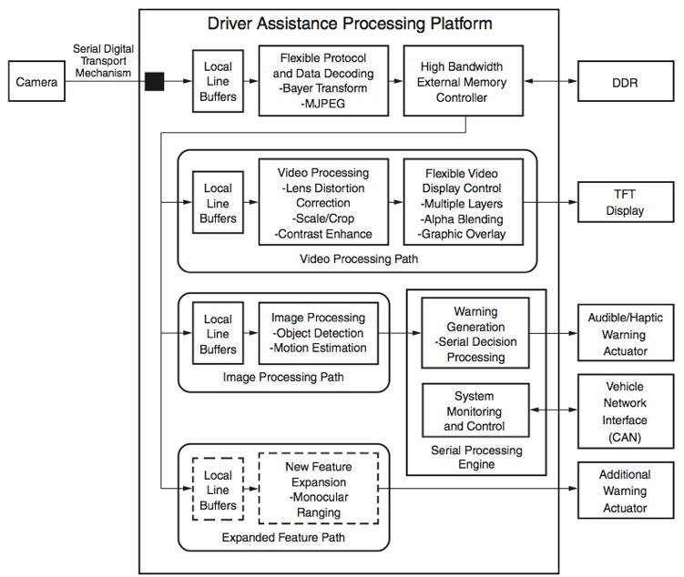
Figure 3. Video and Image Processing Functions
FPGAs offer highly flexible architectures to address various processing strategies. Within the FPGA logic, it is a simple matter to split the camera signal to feed independent video- and image-processing intellectual property (IP) blocks. Unlike serial processor implementations, which must time-multiplex resources across functions, the FPGA can execute and clock processing blocks independently. Additionally, if it becomes necessary to make a change in the processing architecture, the FPGA's ability to reprogram hardware blocks surpasses solutions based on specialized application-specific standard products (ASSPs) and application-specific integrated circuits (ASICs), giving FPGA implementations a large advantage when anticipating the future evolution of advanced algorithms. For computationally intensive processing, FPGA devices, such as the new XA Spartan®-6 FPGA Automotive family, offer up to 180 independent multiply-and-accumulate (MACC) units with pre-adders.
Another benefit of FPGA implementation is device scalability. As OEMs look to bundle more features, the processing needs will rise. For example, the rear-view camera might need to host a monocular ranging algorithm to provide drivers with information on object distance. The added functionality requires yet another parallel-processing path. Implementing this in a specialized ASIC or ASSP could be problematic, if not impossible, unless the designers made provisions for such expansion ahead of time.
Attempting to add this functionality to a serial DSP could require a complete re-architecture of the software design, even after moving to a more powerful device in the family (if it is plausible at all). By contrast, an FPGA-based implementation allows the new functional block to be added, utilizing previously unused FPGA logic and leaving existing blocks virtually intact. Even if the new function requires more resources than are available in the original device, part/package combinations frequently support moving to a denser device (that is, one with more processing resources) without the need to redesign the circuit board or existing IP blocks.
Finally, the reprogrammable nature of the FPGA offers "silicon reuse" for mutually exclusive DA functions. In the rear-looking camera example, the features described are useful while a vehicle is backing up, but an FPGA-based system could leverage the same sensor and processing electronics while the vehicle is moving forward, with a feature like blind-spot detection. In this application, the system analyzes the camera image to determine the location and relative motion of detected objects. Since this feature and its associated processing functions are not required at the same time as the backup feature, the system can reconfigure the FPGA logic within several hundred milliseconds based on the vehicle state. This allows complete reuse of the FPGA device to provide totally different functionality at very little cost.
Meeting DA External Memory Bandwidth Requirements
In addition to raw processing performance, camera-based DA applications require significant external memory access bandwidth. The most stringent requirements come from multi-camera systems with centralized processing, for example, a four-camera surround-view system. Assuming 4 megapixel imagers (1,280 x 960), 24-bit color processing, and performance of 30 frames per second (FPS), just storing the imagers in external buffers requires 3.6 Gb/s of memory access. If the images need to be simultaneously read and written, the requirement doubles to 7.2 Gb/s. With an 80% read/write burst efficiency, the requirement increases to 8.5 Gb/s. This estimate does not include other interim image storage or code access needs. With these requirements, it is clear that camera-based DA applications are memory bandwidth-intensive.
These systems also commonly require memory controllers; however, adding one in a cost-effective manner requires efficient system-level design. Again, developers can leverage the FPGA's flexibility to meet this need. XA Spartan-6 devices offer two hardened memory controller blocks (MCBs) that designers can configure for 4-, 8- or 16-bit DDR, DDR2, DDR3, or LPDDR memory interfaces. They can clock the MCBs at up to 400 MHz, providing 12.8 Gb/s memory access bandwidth to a 16-bit-wide memory device. Furthermore, with two MCBs, the raw bandwidth doubles to 25.6 Gb/s. The two MCBs can run independently or work together using FPGA logic to create a virtual 32-bit-wide data width.
To summarize, FPGA memory controllers provide customized external memory interface design options to meet DA bandwidth needs and optimize all aspects of the cost equation (memory device type, number of PCB layers, etc.).
DA Image Processing Need for On-Chip Memory Resources
In addition to external memory needs, camera-based DA processing can benefit from on-chip memory that serves as line buffers for processing streaming video or analyzing blocks of image data. Bayer transform, lens distortion correction, and optical-flow motion-analysis are examples of functions that require video line buffering. For a brief quantitative analysis, a Bayer transform function using 12-bit-pixel Bayer pattern intensity information to produce 24-bit color data is examined. Implemented as a raw streaming process, a bicubic interpolation process requires buffering four lines of image data. Packing the 12-bit-intensity data into 16-bit locations requires approximately 20.5 kb of storage per line, or 82 kb for four lines of data.
FPGAs provide on-chip memory resources in the form of block RAM. The XA Spartan-6 family has increased the block-RAM-to-logic ratios to support image-processing needs. The XA Spartan-6 devices offer between 216 kb and 4.7 Mb of block RAM memory structured in dual-port 18 kb blocks capable of 320 MHz clocking.
Transporting Video Data over High-Speed Serial Interfaces
Another DA processing platform issue relates to transport of video data from remotely mounted cameras to central processing or display-capable modules. Most of today's camera installations rely on analog composite video transport (for example, NTSC). However, this method presents several problems for advanced DA systems. Interlaced fields can reduce the effectiveness of object-recognition and motion-estimation algorithms, and analog signals are susceptible to electrical noise, which adversely affects image quality. Finally, with the advent of digital imagers, conversion to or from composite video (CVBS) formats can introduce unnecessary system costs.
A preferred method is to use a digital transport mechanism. Transporting 12 bits of data in parallel can be costly in terms of cable and connectors, so serialization techniques involving low-voltage differential signaling (LVDS) or Ethernet technologies are currently under consideration. Serializing pixel data requires the use of devices with high-speed interfaces. A single 30 FPS megapixel imager with 12-bit pixel depth generates data at greater than 500 Mb/s.
XA Spartan-6 devices offer differential I/O that can operate at speeds exceeding 1 Gb/s, and several members of the family also offer serial transceivers that can be clocked at better than 3 Gb/s. It is possible to leverage these high-speed I/O capabilities along with the FPGA logic to implement emerging LVDS SerDes signaling protocols within the FPGA device itself, eliminating external components and reducing system cost.
Functional Partitioning of Parallel and Serial DA Processes
For the single-camera system with rear cross-path warning example, the video- and image-processing functions clearly benefit from parallel processing and hardware acceleration, while the cross-path warning generation is a serial decision process. So a platform that can support both types of processing is clearly an advantage.
Xilinx FPGAs support instantiation of soft processors such as the MicroBlazeTM 32-bit RISC embedded processor, available in XA Spartan-6 devices. Combining full-function processors with FPGA logic allows for optimized functional partitioning i.e., the functions that benefit from parallel processing or hardware acceleration are implemented in FPGA logic, while those more suited for serial processes are implemented in software and executed on the MicroBlaze processor. While the MicroBlaze processor is capable of supporting system-on-chip (SoC) architectures, Xilinx's 7 series devices include an Extensible Processing Platform with hardened ARM® dual core CortexTM-A9 processors along with a hardened set of peripherals. Xilinx is targeting these 7 series devices for the most complex of DA systems.
Conclusion
System designers working on DA processing platforms must consider architectural flexibility, platform scalability, external memory bandwidth, on-chip memory resources, high-speed serial interfaces, and parallel/serial process partitioning. The challenge is to strike an appropriate balance between meeting these needs and maintaining a competitive product cost structure. In this quest, FPGA technology is a viable alternative to standard ASSP and ASIC approaches. In particular, the resource attributes of the XA Spartan-6 family offer unique options and capabilities in meeting the DA processing platform requirements. With today's FPGAs utilizing 40 nm process nodes and 7 series devices moving to 28 nm, their competitive position as a DA processing platform of choice is very strong for some time to come.
To learn more about the XA Spartan-6 family and the benefits it can offer, go to:
For a demonstration of a four camera surround view system based on Spartan-6 FPGAs, go to: