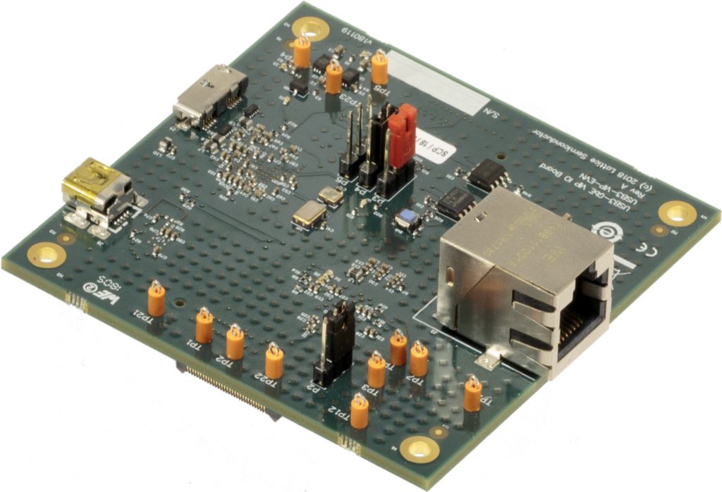
New DisplayPort, eDP, GigE/USB 3.0, HDMI Interface Boards and IPs Complement Award-winning Embedded Vision Development Kit
- Lattice’s Video Interface Platform (VIP) accelerates rapid prototyping with DisplayPort, eDP, USB 3.0, GigE and HDMI® interfaces
- USB3-GigE VIP IO Board provides high-speed video capture for simplified design with the Embedded Vision Development Kit
- IPs from partners Bitec and Helion Vision® support a variety of input and output boards
PORTLAND, OR – May 15, 2018 – Lattice Semiconductor Corporation (NASDAQ: LSCC), the leading provider of customizable smart connectivity solutions, today announced the release of the USB3-GigE VIP IO Board, extending the design interface options with the Video Interface Platform (VIP). Based on Lattice’s award-winning Embedded Vision Development Kit, the VIP platform offers embedded system designers the flexibility of interchangeable input and output boards to simplify connectivity to a broad variety of video interfaces. Newly released USB3-GigE VIP IO Board complements existing VIP offering consisting of the ECP5™ VIP Processor Board, CrossLink™ VIP Input Bridge Board, HDMI VIP Input and HDMI VIP Output Boards, and DisplayPort™ VIP Output and Input Boards.
The modular VIP platform provides designers with the ability to build an embedded vision prototyping system quickly by mixing and matching different input and output boards, eliminating cumbersome manual wiring and enabling faster time-to-market through a unified connector. At the base of the platform is the Embedded Vision Development Kit which combines the benefits of the CrossLink mobile bridging FPGA, the optimized ECP5 image signal processing FPGA, and the high-bandwidth, high-resolution HDMI ASSP onto a single, ready-to-use design platform. Lattice’s new USB3-GigE VIP IO Board enables Ethernet connections at gigabit speeds and USB 3.0 connectivity, extending the VIP interface options, and ensuring simplified prototyping for embedded vision systems.
“With more applications looking to integrate vision technology, Lattice continues to solve designer problems by offering advanced connectivity and the reuse of proven hardware and software building blocks,” said Dirk Seidel, senior product marketing manager at Lattice Semiconductor. “The addition of the USB3-GigE VIP IO Board to our Video Interface Platform, allows designers to simply add network connectivity through the use of a unified connector, accelerating their embedded vision prototyping.”
In addition to a variety of hardware option, Lattice’s VIP offers IPs from 3rd party VIP ecosystem partners. IP options include commercial grade Image Signal Processing and networking stacks, Helion Vision’s GigE Vision, and a variety of different sensor input boards and DisplayPort IP (including eDP support) from Bitec.
For more information about Lattice’s VIP ecosystem and the USB3-GigE board, please visit http://www.latticesemi.com/VIP.
For more information about Lattice’s Embedded Vision Development Kit, please visit http://www.latticesemi.com/en/Products/DevelopmentBoardsAndKits/EmbeddedVisionDevelopmentKit.
Lattice at the Embedded Vision Summit 2018 – Santa Clara, CA
Lattice will be exhibiting at Embedded Vision Summit 2018 in Santa Clara from Tuesday, May 22 to Wednesday, May 23, where members of the Lattice team will showcase some of its latest advancements in Edge connectivity and Edge computing solutions in the Industrial, Automotive, and Consumer markets. To schedule a press meeting, please contact: [email protected]. To schedule a customer meeting, please visit: http://www.latticesemi.com/en/About/ContactUs.aspx.
About Lattice Semiconductor
Lattice Semiconductor (NASDAQ: LSCC) is a leader in smart connectivity solutions at the network edge, where the “things” of IoT live. Our low power FPGA, 60 GHz millimeter wave, video ASSP and IP products deliver edge intelligence, edge connectivity, and control solutions to the consumer, communications, industrial, compute, and automotive markets. Our unwavering commitment to our global customers enables them to accelerate their innovation, creating an ever better and more connected world.
For more information about Lattice please visit www.latticesemi.com. Stay in the know by subscribing to the Lattice newsletter or following us on LinkedIn, Twitter, Facebook, YouTube, WeChat, Weibo or Youku.


