

VeriSilicon

VeriSilicon Introduces CPP2000 Camera Post-Processing IP for Embodied Robotics and Mobile Vision Applications

Shanghai, China, July 3, 2026–VeriSilicon (688521.SH) today announced its high-performance CPP2000 Camera Post-Processing (CPP) IP, expanding the company’s Image Signal Processing (ISP) solutions with advanced post-processing capabilities. By improving image quality and visual perception in mobile imaging scenarios, CPP2000 enables more reliable vision performance in robotics, drones, and other mobile vision applications. CPP2000 integrates multiple […]

VeriSilicon Introduces CPP2000 Camera Post-Processing IP for Embodied Robotics and Mobile Vision Applications Read More +

“One Silicon, Two Worlds: NPU Optimization for Autoregressive and Diffusion Transformers,” a Presentation from VeriSilicon

Shang-Hung Lin, Vice President of NPU Technology at VeriSilicon presents “One Silicon, Two Worlds: NPU Optimization for Autoregressive and Diffusion Transformers” at the May 2026 Embedded Vision Summit. Physical AI is caught between two computational titans: autoregressive (AR) transformers, which predict discrete action tokens, and diffusion transformers (DiTs), which refine… “One Silicon, Two Worlds: NPU

“One Silicon, Two Worlds: NPU Optimization for Autoregressive and Diffusion Transformers,” a Presentation from VeriSilicon Read More +

VeriSilicon Demonstration of a Partner Application In the iEVCam

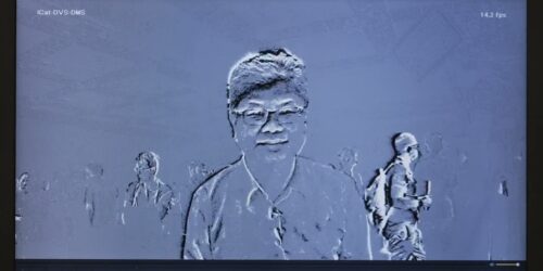
Halim Theny, VP of Product Engineering at VeriSilicon, demonstrates the company’s latest edge AI and vision technologies and products at the 2025 Embedded Vision Summit. Specifically, Theny demonstrates a customer’s SoC, featuring a collaboration with a premier camera vendor using an event-based sensor to detect motion, and processed by VeriSilicon’s NPU and vision DSP. This

VeriSilicon Demonstration of a Partner Application In the iEVCam Read More +

VeriSilicon Demonstration of the Open Se Cura Project

Chris Wang, VP of Multimedia Technologies and a member of CTO office at VeriSilicon, demonstrates the company’s latest edge AI and vision technologies and products at the 2025 Embedded Vision Summit. Specifically, Wang demonstrates examples from the Open Se Cura Project, a joint effort between VeriSilicon and Google. The project showcases a scalable, power-efficient, and

VeriSilicon Demonstration of the Open Se Cura Project Read More +

VeriSilicon Demonstration of Advanced AR/VR Glasses Solutions

Dr. Mahadev Kolluru, Senior VP of North America and India Business at VeriSilicon, demonstrates the company’s latest edge AI and vision technologies and products at the 2025 Embedded Vision Summit. Specifically, Dr. Kolluru demonstrates products developed using the company’s IP licensing and turnkey silicon design services. Dr. Kolluru highlights how VeriSilicon supports cutting-edge AI and

VeriSilicon Demonstration of Advanced AR/VR Glasses Solutions Read More +

VeriSilicon Expands DSP Portfolio with Silicon-proven ZSP5000 Vision Core Series for Edge Intelligence

Highly scalable architecture optimized for computer vision and image workloads with extendable instruction set Shanghai, China, June 26, 2025–VeriSilicon (688521.SH) today released the ZSP5000 Digital Signal Processing (DSP) series IPs, which are based on its fifth-generation silicon-proven DSP architecture. This product line adopts a highly scalable and energy-efficient design, and has been deeply optimized for

VeriSilicon Expands DSP Portfolio with Silicon-proven ZSP5000 Vision Core Series for Edge Intelligence Read More +

“Image Tokenization for Distributed Neural Cascades,” a Presentation from Google and VeriSilicon

Derek Chow, Software Engineer at Google, and Shang-Hung Lin, Vice President of NPU Technology at VeriSilicon, co-present the “Image Tokenization for Distributed Neural Cascades” tutorial at the May 2025 Embedded Vision Summit. Multimodal LLMs promise to bring exciting new abilities to devices! As we see foundational models become more capable, we see compute requirements grow

“Image Tokenization for Distributed Neural Cascades,” a Presentation from Google and VeriSilicon Read More +

VeriSilicon’s Ultra-low Energy NPU Provides Over 40 TOPS for On-device LLM Inference in Mobile Applications

The energy-efficient architecture scales across AI-enabled devices, including AI phones and AI PCs Shanghai, China, June 9, 2025–VeriSilicon (688521.SH) today announced that its ultra-low energy and high-performance Neural Network Processing Unit (NPU) IP now supports on-device inference of large language models (LLMs) with AI computing performance scaling beyond 40 TOPS. This energy-efficient NPU architecture is

VeriSilicon’s Ultra-low Energy NPU Provides Over 40 TOPS for On-device LLM Inference in Mobile Applications Read More +

VeriSilicon’s Scalable High-performance GPGPU-AI Computing IPs Empower Automotive and Edge Server AI Solutions

Provide AI acceleration with high computing density, multi-chip scaling, and 3D-stacked memory integration Shanghai, China, June 9, 2025–VeriSilicon (688521.SH) today announced the latest advancements in its high-performance and scalable GPGPU-AI computing IPs, which are now empowering next-generation automotive electronics and edge server applications. Combining programmable parallel computing with a dedicated Artificial Intelligence (AI) accelerator, these

VeriSilicon’s Scalable High-performance GPGPU-AI Computing IPs Empower Automotive and Edge Server AI Solutions Read More +

VeriSilicon’s AI-ISP Custom Chip Solution Enables Mass Production of Customer’s Smartphones

Providing architecture design, software-hardware co-development, and mass production support, and enhancing AI-powered imaging capabilities in smart devices Shanghai, China, June 9, 2025–VeriSilicon (688521.SH) recently announced that its AI-ISP custom chip solution has been successfully adopted in a customer’s mass-produced smartphones, reaffirming the company’s comprehensive one-stop custom silicon service capabilities in AI vision processing. VeriSilicon’s AI-ISP

VeriSilicon’s AI-ISP Custom Chip Solution Enables Mass Production of Customer’s Smartphones Read More +

Here you’ll find a wealth of practical technical insights and expert advice to help you bring AI and visual intelligence into your products without flying blind.

Contact

Address

Berkeley Design Technology, Inc.
PO Box #4446
Walnut Creek, CA 94596

Phone
Phone: +1 (925) 954-1411
Scroll to Top