
The Coming Robotics Revolution: How AI and Macnica’s Capture, Process, Communicate Philosophy Will Define the Next Industrial Era
This blog post was originally published at Macnica’s website. It is reprinted here with the permission of Macnica. Just as networking and fiber-optic infrastructure quietly laid the groundwork for the internet economy, fueling the rise of Amazon, Facebook, and the digital platforms that redefined commerce and communication, today’s breakthroughs in artificial intelligence are setting the stage

Red Light Cameras vs. Traffic Sensors: The Ultimate Guide for Traffic Enforcement
This blog post was originally published at e-con Systems’ website. It is reprinted here with the permission of e-con Systems. Intersections create the toughest mix of crashes, congestion, and violations, so cities rely on imaging to bring order and proof. Red light cameras and traffic sensors operate in the same geography yet serve different goals,
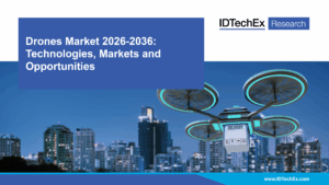
Drones Market 2026-2036: Technologies, Markets, and Opportunities
This article was originally published at IDTechEx’s website. It is reprinted here with the permission of IDTechEx. Global Drone Market Set to Reach US$147.8 Billion by 2036, Driven by Commercial Expansion, Regulatory Maturity, and Sensor Proliferation Over the past decade, drones have moved from experimental tools into critical infrastructure across agriculture, logistics, energy, security, and public-sector
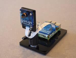
poLight ASA Collaborates with Image Quality Labs on M12-based Raspberry Pi TLens Studio for AI-driven Industrial Machine Vision Applications
TØNSBERG, Norway–(BUSINESS WIRE) — poLight ASA (OSE: PLT) and Image Quality Labs (IQL) today announced the development of an M12-based Raspberry Pi TLens® Studio evaluation and development platform, utilizing the new line of TLens® off-the-shelf (OTS) focusing camera lens. This platform enables machine vision design engineers to quickly and easily evaluate high speed, constant field-of-view
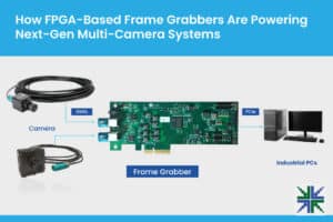
How FPGA-Based Frame Grabbers Are Powering Next-Gen Multi-Camera Systems
This article was originally published at e-con Systems’ website. It is reprinted here with the permission of e-con Systems. FPGA-based frame grabbers are redefining multi-camera vision by enabling synchronized aggregation of up to eight GMSL streams for autonomous driving, robotics, and industrial automation. They overcome bandwidth and latency limits of USB and Ethernet by using PCIe

What is a Dust Denoising Filter in TOF Camera, and How Does it Remove Noise Artifacts in Vision Systems?
This article was originally published at e-con Systems’ website. It is reprinted here with the permission of e-con Systems. Time-of-Flight (ToF) cameras with IR sensors are susceptible to performance variations caused by environmental dust. This dust can create ‘dust noise’ in the output depth map, directly impacting camera accuracy and, consequently, the reliability of critical

e-con Systems to Launch Darsi Pro, an NVIDIA Jetson-Powered AI Compute Box for Advanced Vision Applications
This blog post was originally published at e-con Systems’ website. It is reprinted here with the permission of e-con Systems. This blog offers expert insights into Darsi Pro, how it delivers a unified vision solution, and what it brings to alleviate modern workloads. Darsi Pro comes with GMSL camera options, rugged design, OTA support, and
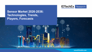
New IDTechEx Report: Sensor Market 2026-2036
This article was originally published at IDTechEx’s website. It is reprinted here with the permission of IDTechEx. IDTechEx forecasts that the global sensor market will reach US$250B by 2036 as global mega-trends in mobility, AI, robotics, 6G connectivity and IoT drive sensor demand. IDTechEx’s newly updated “Sensor Market 2026-2036: Technologies, Trends, Players, Forecasts” report provides extensive
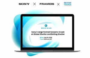
Sony’s Large Format Sensors: A Look at Global Shutter and Rolling Shutter
On December 4, 2025, at 10:00 am CET (4:00 am EST) Alliance Member companies Sony and RESTAR FRAMOS will deliver a 30-minute technical session “Sony’s Large Format Sensors: A Look at Global Shutter and Rolling Shutter” From the event page: Join experts from Sony, FRAMOS, and RESTAR FRAMOS for a focused, 30-minute technical session examining
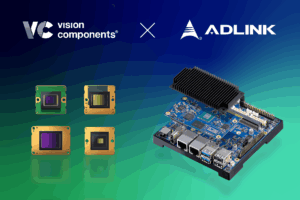
VC MIPI Cameras & ADLINK i.MX 8M Plus: Full Driver Support
Ettlingen, November 18, 2025 — For a medical imaging project, ADLINK wanted to integrate VC MIPI Cameras with its I-Pi SMARC IMX8M Plus Development Kit. Vision Components adapted the standard driver for the NXP i.MX 8M Plus processor platform to the ADLINK board, including full ISP support, for features such as color tuning etc. As