Smart Sensor Demo: On-Device Object Detection with Lattice CertusPro™-NX
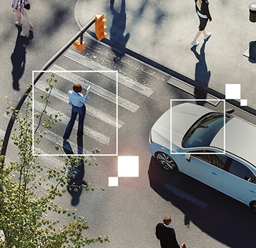
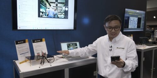
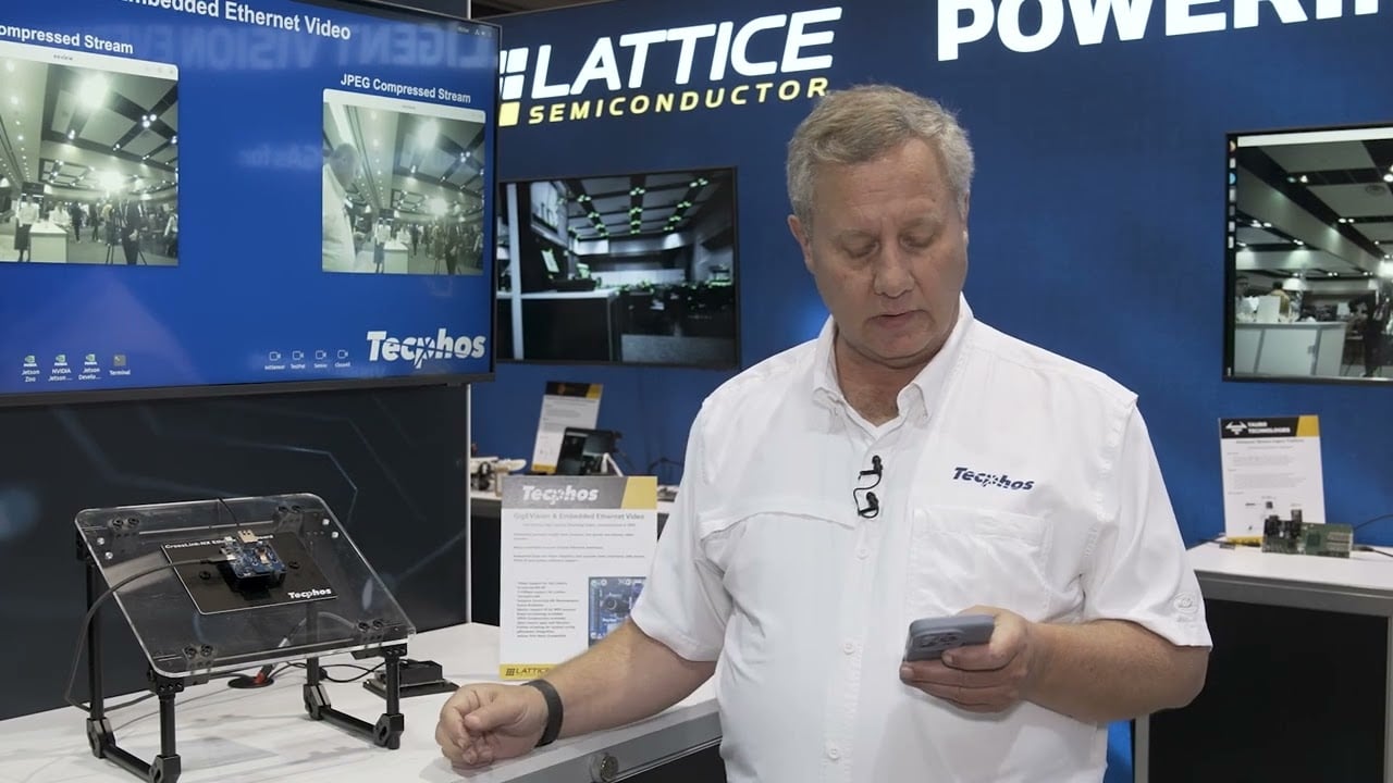
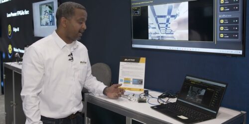
Lattice Semiconductor demonstrates how the CertusPro-NX FPGA bridges an image sensor to a Raspberry Pi, performing on-device pre-processing and object detection before passing data to the host CPU. Sensor frames at 30 fps are fed into the FPGA, where an object detection model — trained on eight automotive object classes — runs locally and outputs […]
Smart Sensor Demo: On-Device Object Detection with Lattice CertusPro™-NX Read More +